SNVS872D August   2012  – August 2018 LMZ21700

PRODUCTION DATA.  

  1. Features
  2. Applications
  3. Description
    1.     Device Images
      1.      Simplified Schematic
      2.      Efficiency for VIN = 12 V
  4. Revision History
  5. Pin Configuration and Functions
    1.     Pin Functions
  6. Specifications
    1. 6.1 Absolute Maximum Ratings
    2. 6.2 ESD Ratings
    3. 6.3 Recommended Operating Conditions
    4. 6.4 Thermal Information
    5. 6.5 Electrical Characteristics
    6. 6.6 Typical Characteristics
  7. Detailed Description
    1. 7.1 Overview
    2. 7.2 Functional Block Diagram
      1. 7.2.1 Package Construction
    3. 7.3 Feature Description
      1. 7.3.1 Input Undervoltage Lockout
      2. 7.3.2 Enable Input (EN)
      3. 7.3.3 Soft-Start and Tracking Function (SS)
      4. 7.3.4 Power Good Function (PG)
      5. 7.3.5 Output Voltage Setting
      6. 7.3.6 Output Current Limit and Output Short Circuit Protection
      7. 7.3.7 Thermal Protection
    4. 7.4 Device Functional Modes
      1. 7.4.1 PWM Mode Operation
      2. 7.4.2 PSM Operation
  8. Application and Implementation
    1. 8.1 Application Information
    2. 8.2 Typical Application
      1. 8.2.1 Design Requirements
      2. 8.2.2 Detailed Design Procedure
        1. 8.2.2.1 Custom Design With WEBENCH® Tools
        2. 8.2.2.2 Input Capacitor (CIN)
        3. 8.2.2.3 Output Capacitor (COUT)
        4. 8.2.2.4 Softstart Capacitor (CSS)
        5. 8.2.2.5 Power Good Resistor (RPG)
        6. 8.2.2.6 Feedback Resistors (RFBB and RFBT)
      3. 8.2.3 Application Curves
        1. 8.2.3.1 VOUT = 1.2 V
        2. 8.2.3.2 VOUT = 1.8 V
        3. 8.2.3.3 VOUT = 2.5 V
        4. 8.2.3.4 VOUT = 3.3 V
        5. 8.2.3.5 VOUT = 5.0 V
    3. 8.3 Do's and Don'ts
  9. Power Supply Recommendations
    1. 9.1 Voltage Range
    2. 9.2 Current Capability
    3. 9.3 Input Connection
      1. 9.3.1 Voltage Drops
      2. 9.3.2 Stability
  10. 10Layout
    1. 10.1 Layout Guidelines
      1. 10.1.1 Minimize the High di/dt Loop Area
      2. 10.1.2 Protect the Sensitive Nodes in the Circuit
      3. 10.1.3 Provide Thermal Path and Shielding
    2. 10.2 Layout Example
      1. 10.2.1 High Density Layout Example for Space Constrained Applications
        1. 10.2.1.1 35-mm² Solution Size (Single Sided)
  11. 11Device and Documentation Support
    1. 11.1 Device Support
    2. 11.2 Development Support
      1. 11.2.1 Custom Design With WEBENCH® Tools
    3. 11.3 Receiving Notification of Documentation Updates
    4. 11.4 Community Resources
    5. 11.5 Trademarks
    6. 11.6 Electrostatic Discharge Caution
    7. 11.7 Glossary
  12. 12Mechanical, Packaging, and Orderable Information
    1. 12.1 Tape and Reel Information

Package Options

Refer to the PDF data sheet for device specific package drawings

Mechanical Data (Package|Pins)
  • SIL|8
Thermal pad, mechanical data (Package|Pins)
Orderable Information

VOUT = 3.3 V

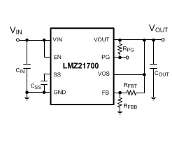
LMZ21700 TYP_SCH_00.gifFigure 56. Typical Applications Circuit
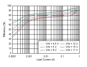
LMZ21700 D019_LMZ21700_25C_3.3VOUT_EFFICIENCY_LOG_SNVS872.gifFigure 58. Efficiency VOUT = 3.3 V
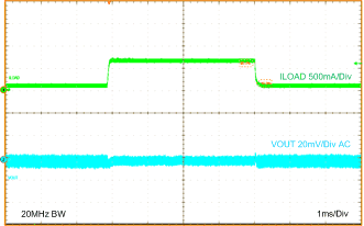
LMZ21700 LMZ21700_3.3VOUT_LOAD_TRANS_100mA_to_650mA_snvs872.gifFigure 60. Load Transient VOUT = 3.3 V
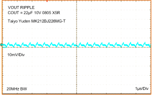
LMZ21700 LMZ21700_3.3VOUT_RIPPLE_20MHzBW_snvs872.gifFigure 62. 20 MHz Oscilloscope Bandwidth
Output Voltage Ripple VOUT = 3.3 V
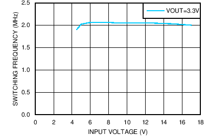
LMZ21700 LMZ21700_FSW_3.3VOUT_snvs872.pngFigure 64. Typical Switching Frequency at 650mA Load VOUT = 3.3 V
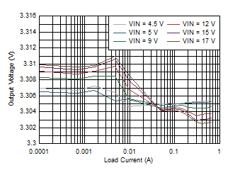
LMZ21700 D020_LMZ21700_25C_3.3VOUT_LINE_AND_LOAD_REG_LOG_SNVS872.gifFigure 66. Line and Load Regulation VOUT = 3.3 V
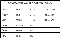
LMZ21700 3.3V_BOM_snvs872.gifFigure 57. External Component Values
(VOUT = 3.3V)
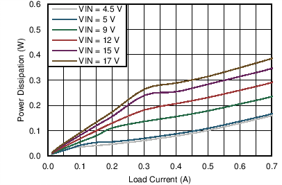
LMZ21700 LMZ21700_25C_3.3VOUT_POWER_DISSIPATION_snvs872.pngFigure 59. Power Dissipation VOUT = 3.3 V
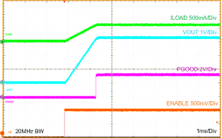
LMZ21700 LMZ21700_3.3VOUT_STARTUP_snvs872.gifFigure 61. Startup VOUT = 3.3 V
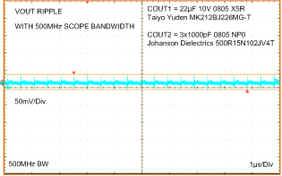
LMZ21700 LMZ21700_3.3VOUT_RIPPLE_500MHzBW_snvs872.gifFigure 63. 500MHz Oscilloscope Bandwidth, 3x1000 pF additional output capacitance
Output Voltage Ripple and HF Noise VOUT = 3.3 V
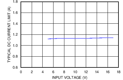
LMZ21700 LMZ21700_ICL_3.3V_85C_snvs872.pngFigure 65. Typical Current Limit VOUT = 3.3 V, TA = 85 °C
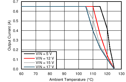
LMZ21700 LMZ21700SIL_3.3VO_47CperW_snvs872.pngFigure 67. Thermal Derating for θJA = 47ºC/W, VOUT = 3.3 V