SLVS582I April 2006 – November 2014 LP2950 , LP2951
PRODUCTION DATA.
- 1 Features
- 2 Applications
- 3 Description
- 4 Revision History
- 5 Pin Configuration and Functions
- 6 Specifications
- 7 Detailed Description
- 8 Application and Implementation
- 9 Power Supply Recommendations
- 10Layout
- 11Device and Documentation Support
- 12Mechanical, Packaging, and Orderable Information
Package Options
Mechanical Data (Package|Pins)
Thermal pad, mechanical data (Package|Pins)
- DRG|8
Orderable Information
7 Detailed Description
7.1 Overview
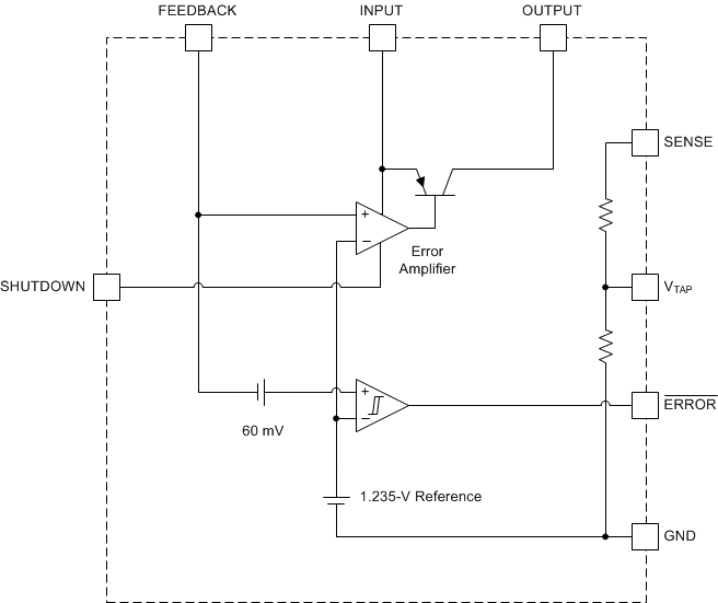
The LP2950 and LP2951 devices are bipolar, low-dropout voltage regulators that can accommodate a wide input supply-voltage range of up to 30 V. The easy-to-use, 3-pin LP2950 is available in fixed-output voltages of 5 V, 3.3 V, and 3 V. However, the 8-pin LP2951 device is able to output either a fixed or adjustable output from the same device. By tying the OUTPUT and SENSE pins together, and the FEEDBACK and VTAP pins together, the LP2951 device outputs a fixed 5 V, 3.3 V, or 3 V (depending on the version). Alternatively, by leaving the SENSE and VTAP pins open and connecting FEEDBACK to an external resistor divider, the output can be set to any value between 1.235 V to 30 V.
The 8-pin LP2951 device also offers additional functionality that makes it particularly suitable for battery-powered applications. For example, a logic-compatible shutdown feature allows the regulator to be put in standby mode for power savings. In addition, there is a built-in supervisor reset function in which the ERROR output goes low when VOUT drops by 6% of its nominal value for whatever reasons – due to a drop in VIN, current limiting, or thermal shutdown.
The LP2950 and LP2951 devices are designed to minimize all error contributions to the output voltage. With a tight output tolerance (0.5% at 25°C), a very low output voltage temperature coefficient (20 ppm typical), extremely good line and load regulation (0.3% and 0.4% typical), and remote sensing capability, the parts can be used as either low-power voltage references or 100-mA regulators.
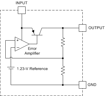
7.2 LP2950 Functional Block Diagram
7.3 LP2951 Functional Block Diagram
7.4 Feature Description
7.4.1 ERROR Function (LP2951 Only)
The LP2951 device has a low-voltage detection comparator that outputs a logic low when the output voltage drops by ≈6% from its nominal value, and outputs a logic high when VOUT has reached ≈95% of its nominal value. This 95% of nominal figure is obtained by dividing the built-in offset of ≈60 mV by the 1.235-V bandgap reference, and remains independent of the programmed output voltage. For example, the trip-point threshold (ERROR output goes high) typically is 4.75 V for a 5-V output and 11.4 V for a 12-V output. Typically, there is a hysteresis of 15 mV between the thresholds for high and low ERROR output.
A timing diagram is shown in Figure 31 for ERROR vs VOUT (5 V), as VIN is ramped up and down. ERROR becomes valid (low) when VIN ≈ 1.3 V. When VIN ≈ 5 V, VOUT = 4.75 V, causing ERROR to go high. Because the dropout voltage is load dependent, the output trip-point threshold is reached at different values of VIN, depending on the load current. For instance, at higher load current, ERROR goes high at a slightly higher value of VIN, and vice versa for lower load current. The output-voltage trip point remains at ~4.75 V, regardless of the load. Note that when VIN ≤ 1.3 V, the ERROR comparator output is turned off and pulled high to its pullup voltage. If VOUT is used as the pullup voltage, rather than an external 5-V source, ERROR typically is ~1.2 V. In this condition, an equal resistor divider (10 kΩ is suitable) can be tied to ERROR to divide down the voltage to a valid logic low during any fault condition, while still enabling a logic high during normal operation.
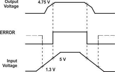 Figure 31. ERROR Output Timing
Because the ERROR comparator has an open-collector output, an external pullup resistor is required to pull the output up to VOUT or another supply voltage (up to 30 V). The output of the comparator is rated to sink up to 400 μA. A suitable range of values for the pullup resistor is from 100 kΩ to 1 MΩ. If ERROR is not used, it can be left open.
7.4.2 Programming Output Voltage (LP2951 Only)
A unique feature of the LP2951 device is its ability to output either a fixed voltage or an adjustable voltage, depending on the external pin connections. To output the internally programmed fixed voltage, tie the SENSE pin to the OUTPUT pin and the FEEDBACK pin to the VTAP pin. Alternatively, a user-programmable voltage ranging from the internal 1.235-V reference to a 30-V max can be set by using an external resistor divider pair. The resistor divider is tied to VOUT, and the divided-down voltage is tied directly to FEEDBACK for comparison against the internal 1.235-V reference. To satisfy the steady-state condition in which its two inputs are equal, the error amplifier drives the output to equal Equation 1:
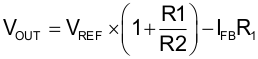
Where:
VREF = 1.235 V applied across R2 (see Figure 32)
IFB = FEEDBACK bias current, typically 20 nA
A minimum regulator output current of 1 μA must be maintained. Thus, in an application where a no-load condition is expected (for example, CMOS circuits in standby), this 1-μA minimum current must be provided by the resistor pair, effectively imposing a maximum value of R2 = 1.2 MΩ (1.235 V/1.2 MΩ ≉ 1 μA).
IFB = 20 nA introduces an error of ≉0.02% in VOUT. This can be offset by trimming R1. Alternatively, increasing the divider current makes IFB less significant, thus, reducing its error contribution. For instance, using
R2 = 100 kΩ reduces the error contribution of IFB to 0.17% by increasing the divider current to ≉12 μA. This increase in the divider current still is small compared to the 600-μA typical quiescent current of the LP2951 under no load.
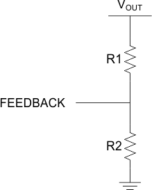 Figure 32. Adjusting the Feedback on the LP2951
7.5 Device Functional Modes
7.5.1 Shutdown Mode
These devices can be placed in shutdown mode with a logic high at the SHUTDOWN pin. Return the logic level low to restore operation or tie SHUTDOWN to ground if the feature is not being used.