SLVS582I April 2006 – November 2014 LP2950 , LP2951
PRODUCTION DATA.
- 1 Features
- 2 Applications
- 3 Description
- 4 Revision History
- 5 Pin Configuration and Functions
- 6 Specifications
- 7 Detailed Description
- 8 Application and Implementation
- 9 Power Supply Recommendations
- 10Layout
- 11Device and Documentation Support
- 12Mechanical, Packaging, and Orderable Information
Package Options
Mechanical Data (Package|Pins)
Thermal pad, mechanical data (Package|Pins)
- DRG|8
Orderable Information
5 Pin Configuration and Functions
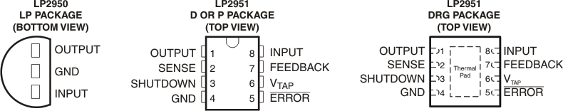
Pin Functions
| PIN | TYPE | DESCRIPTION | ||
|---|---|---|---|---|
| NAME | LP2950 | LP2951 | ||
| ERROR | — | 5 | O | Active-low open-collector error output. Goes low when VOUT drops by 6% of its nominal value. |
| FEEDBACK | — | 7 | I | Determines the output voltage. Connect to VTAP (with OUTPUT tied to SENSE) to output the fixed voltage corresponding to the part version, or connect to a resistor divider to adjust the output voltage. |
| GND | 2 | 4 | — | Ground |
| INPUT | 3 | 8 | I | Supply input |
| OUTPUT | 1 | 1 | O | Voltage output. |
| SENSE | — | 2 | I | Senses the output voltage. Connect to OUTPUT (with FEEDBACK tied to VTAP) to output the voltage corresponding to the part version. |
| SHUTDOWN | — | 3 | I | Active-high input. Shuts down the device. |
| VTAP | — | 6 | O | Tie to FEEDBACK to output the fixed voltage corresponding to the part version. |