SNVS170D October 2001 – April 2016 LP2983
PRODUCTION DATA.
- 1 Features
- 2 Applications
- 3 Description
- 4 Revision History
- 5 Pin Configuration and Functions
- 6 Specifications
- 7 Detailed Description
- 8 Application and Implementation
- 9 Power Supply Recommendations
- 10Layout
- 11Device and Documentation Support
- 12Mechanical, Packaging, and Orderable Information
Package Options
Mechanical Data (Package|Pins)
- DBV|5
Thermal pad, mechanical data (Package|Pins)
Orderable Information
1 Features
- Operating Input Supply Voltage: 2.2 V to 16 V
- Output Current: 150 mA
- Low ZOUT: 0.3 Ω Typical (10 Hz to 1 MHz)
- Stable with Low-ESR Output Capacitor
- Low Ground Pin Current at All Loads
- Output Voltage Accuracy 1% (A Grade)
- High Peak Current Capability
- Wide Supply Voltage Range (16 V Maximum)
- Overtemperature and Overcurrent Protection
- −40°C to +125°C Junction Temperature Range
- Requires Minimum External Components
2 Applications
- Cellular Phones
- Palmtop/Laptop Computers
- Personal Digital Assistants (PDA)
- Camcorders, Personal Stereos, Cameras
3 Description
The LP2983 is a 150-mA, fixed-output voltage regulator designed to provide tight voltage regulation in applications with output voltages ≤ 1.2 V.
Using an optimized vertically integrated PNP (VIP) process, the LP2983 delivers unequaled performance in all critical specifications:
- Ground pin current: Typically 825 µA at a 150-mA load, and 75 µA at a 1-mA load.
- Enhanced stability: The LP2983 is stable with output capacitor ESR down to zero, which allows the use of ceramic capacitors on the output.
- Precision output: 1% tolerance output voltages available (A grade).
- Smallest possible size: SOT-23 package uses absolute minimum board space.
Device Information(1)
| PART NUMBER | PACKAGE | BODY SIZE (NOM) |
|---|---|---|
| LP2983 | SOT-23 (5) | 2.90 mm × 1.60 mm |
- For all available packages, see the orderable addendum at the end of the data sheet.
space
space
space
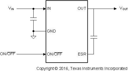
Typical Application
