SNVS482F January 2007 – December 2015
PRODUCTION DATA.
- 1 Features
- 2 Applications
- 3 Description
- 4 Revision History
- 5 Pin Configuration and Functions
- 6 Specifications
- 7 Detailed Description
- 8 Application and Implementation
- 9 Power Supply Recommendations
- 10Layout
- 11Device and Documentation Support
- 12Mechanical, Packaging, and Orderable Information
Package Options
Mechanical Data (Package|Pins)
Thermal pad, mechanical data (Package|Pins)
Orderable Information
8 Application and Implementation
NOTE
Information in the following applications sections is not part of the TI component specification, and TI does not warrant its accuracy or completeness. TI’s customers are responsible for determining suitability of components for their purposes. Customers should validate and test their design implementation to confirm system functionality.
8.1 Application Information
The typical applications of the LP38852-ADJ include DSP supply, microcontroller supplies, and post regulators.
8.2 Typical Application
Figure 23 shows the typical application circuit for LP38852-ADJ.
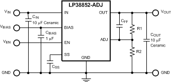 Figure 23. LP38852-ADJ Typical Application
8.2.1 Design Requirements
For typical linear regulator applications, use the parameters listed in Table 2.
Table 2. Design Parameters
| DESIGN PARAMETER | EXAMPLE VALUE |
|---|---|
| Input voltage | 3.3 V |
| Adjustable output voltage | 0.8 V to 1.8 V |
| Output current | 1.5 A |
8.2.2 Detailed Design Procedure
8.2.2.1 External Capacitors
To assure regulator stability, input and output capacitors are required as shown in the Figure 23.
8.2.2.1.1 Input Capacitor
The input capacitor must be at least 10 µF, but can be increased without limit. Its purpose is to provide a low source impedance for the regulator input. A ceramic capacitor, X5R or X7R, is recommended.
Tantalum capacitors may also be used at the input pin. There is no specific equivalent series resistance (ESR) limitation on the input capacitor (the lower, the better).
Aluminum electrolytic capacitors can be used, but are not recommended as their ESR increases very quickly at cold temperatures. They are not recommended for any application where the ambient temperature falls below 0°C.
8.2.2.1.2 Output Capacitor
A minimum output capacitance of 10 µF, ceramic, is required for stability. The amount of output capacitance can be increased without limit. The output capacitor must be located less than 1 cm from the output pin of the device and returned to the device ground pin with a clean analog ground.
Only high-quality ceramic types such as X5R or X7R are recommended, as the Z5U and Y5F types do not provide sufficient capacitance over temperature.
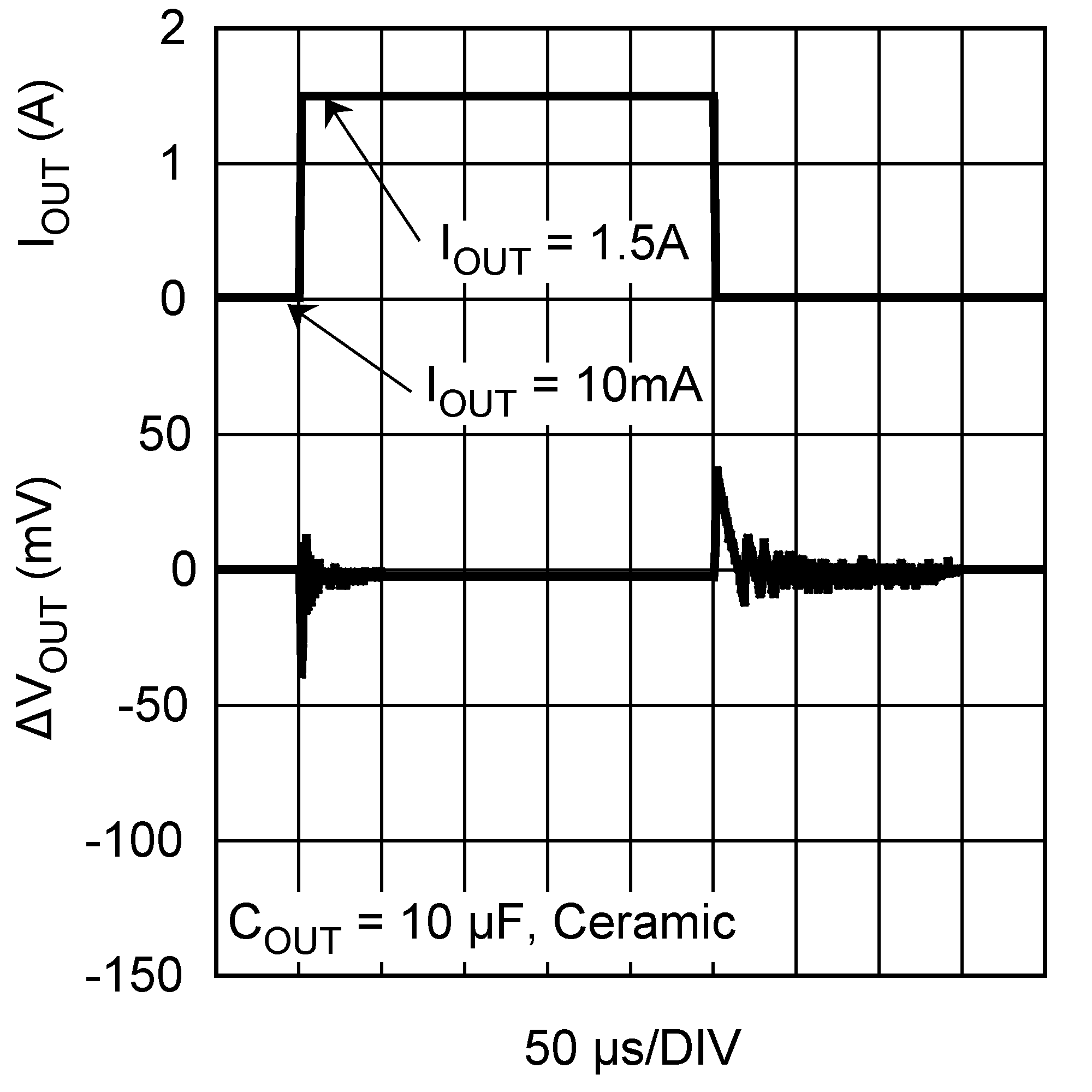
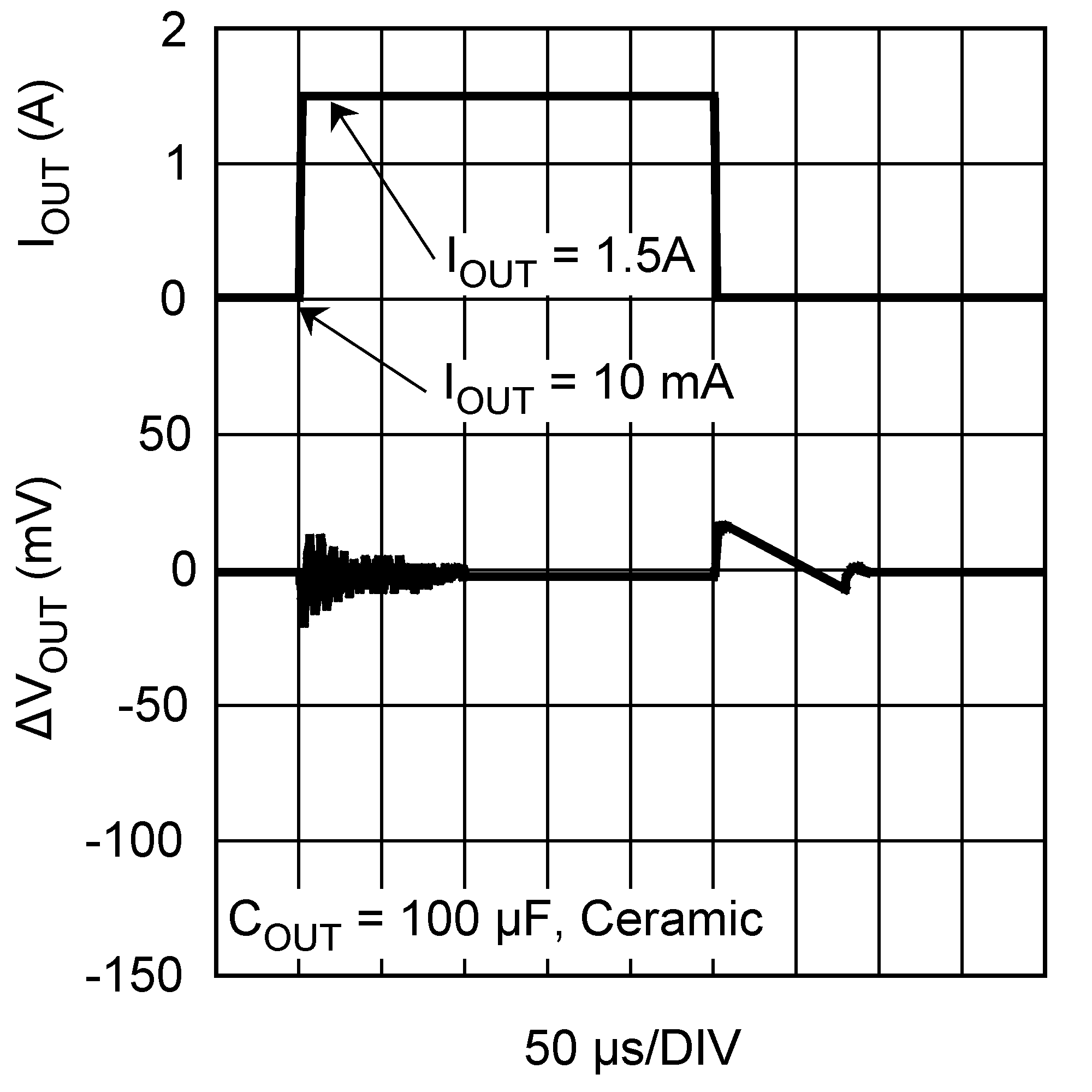
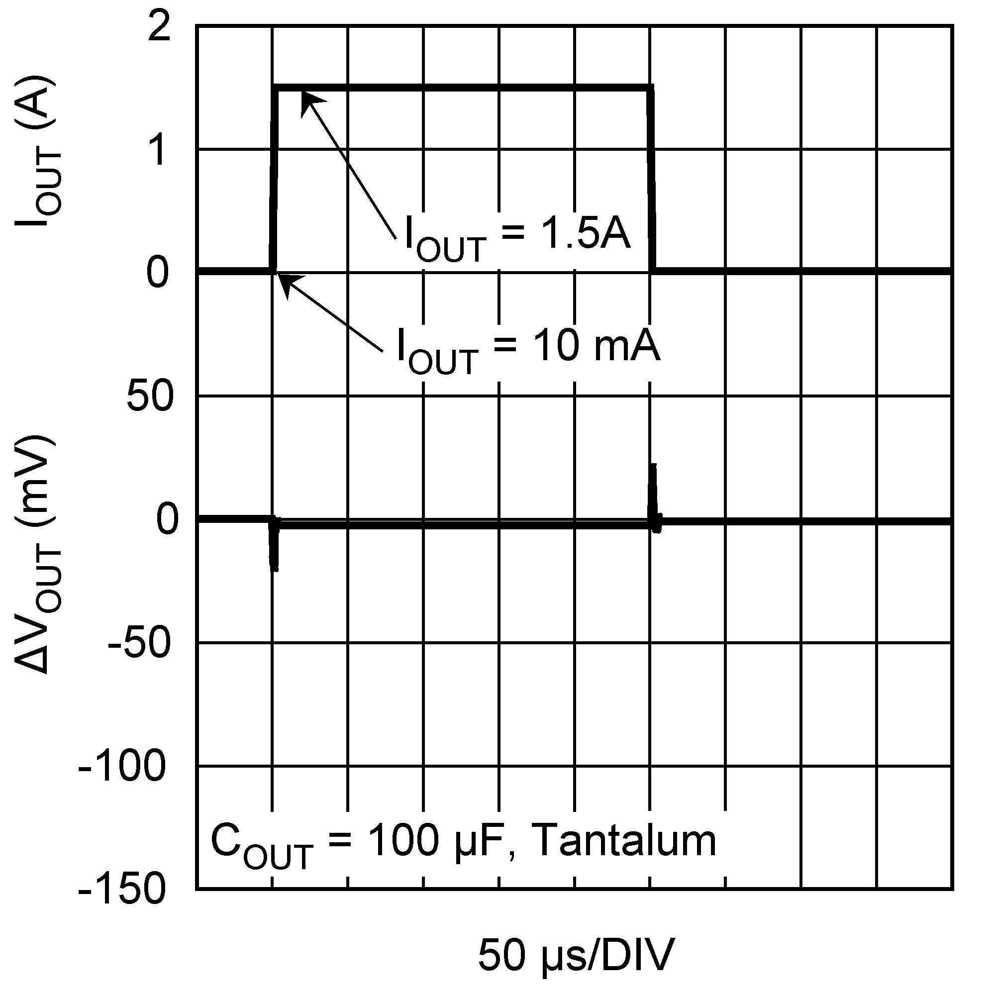
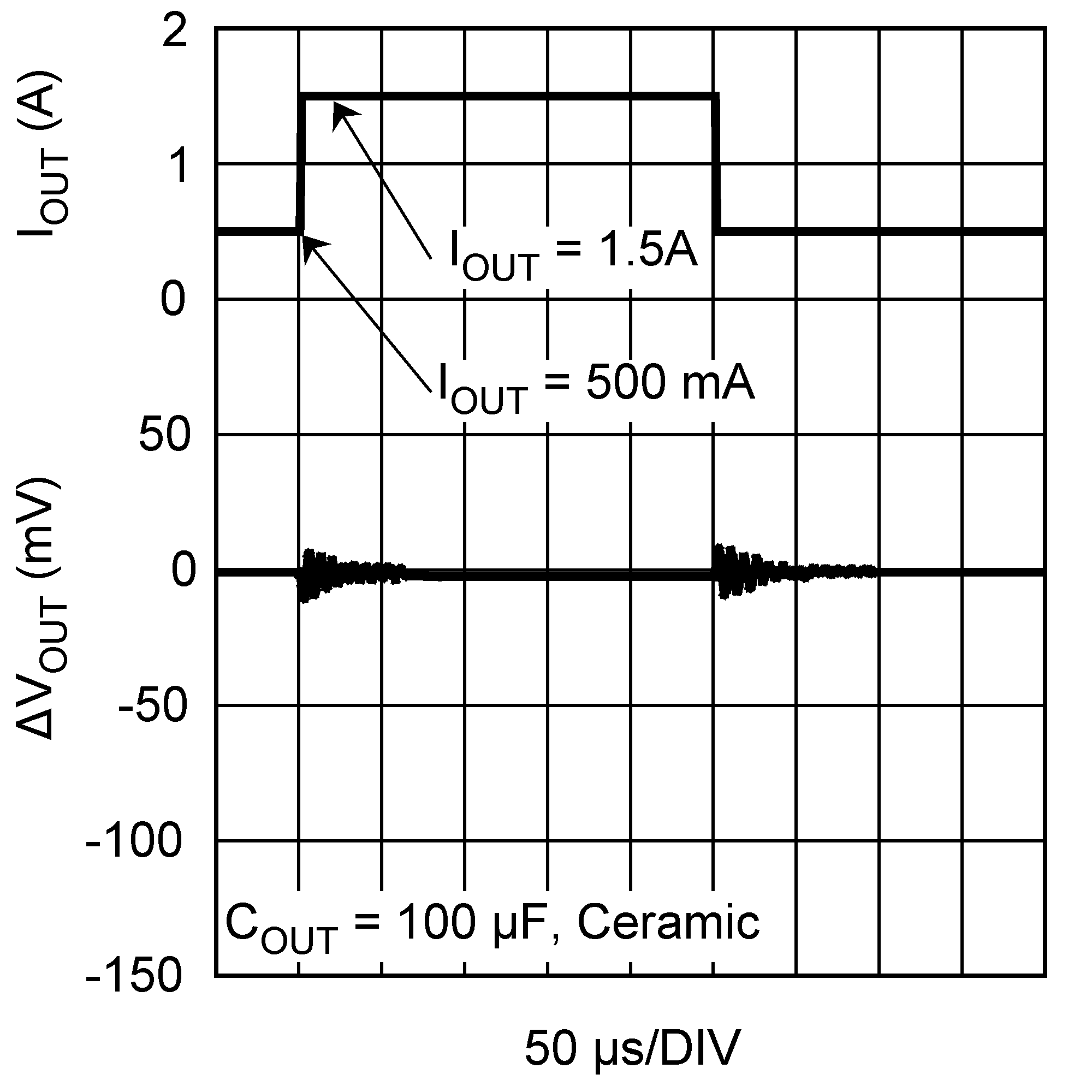
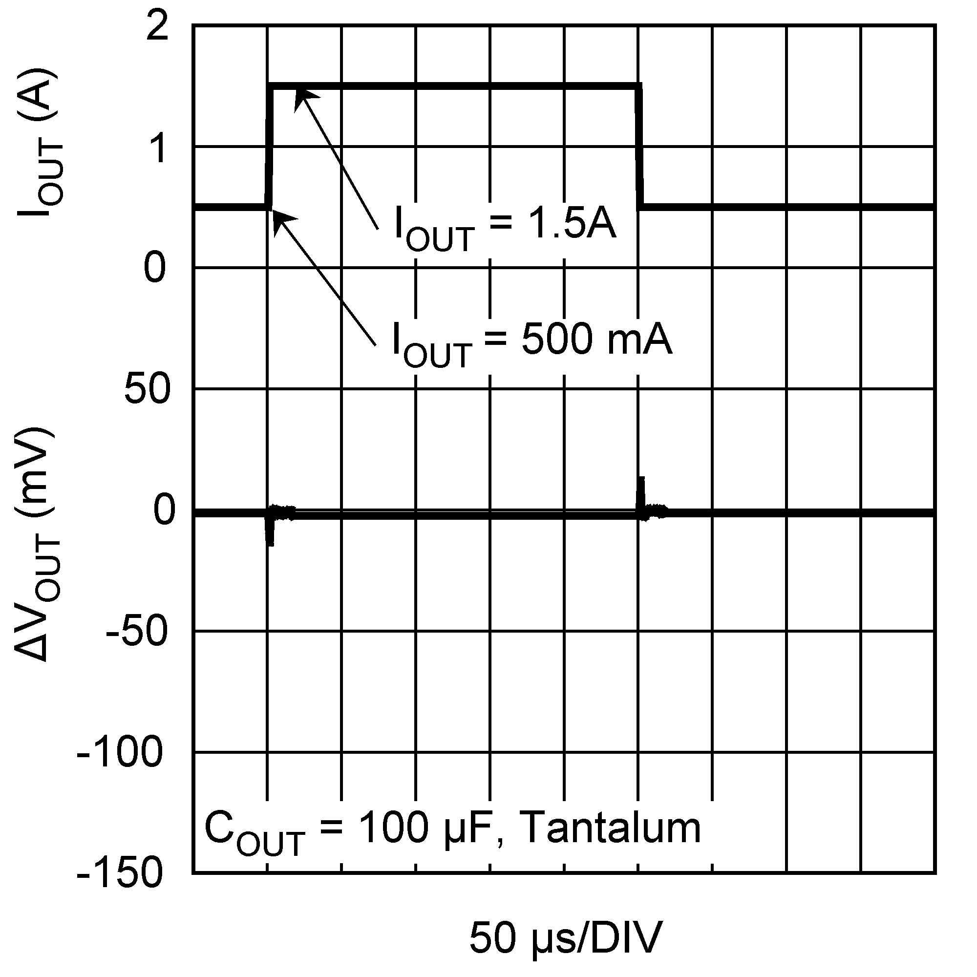
Tantalum capacitors also provide stable operation across the entire operating temperature range. However, the effects of ESR may provide variations in the output voltage during fast load transients. Using the minimum recommended 10-µF ceramic capacitor at the output allows unlimited capacitance, tantalum or aluminum, to be added in parallel.
8.2.2.1.3 Bias Capacitor
The capacitor on the bias pin must be at least 1 µF and can be any good-quality capacitor (ceramic is recommended).
8.2.2.1.4 Setting the Output Voltage
According to Table 1, R1 is set to 1.07 kΩ, and R2 is set to 1.78 kΩ.
8.2.2.1.5 Feed Forward Capacitor, CFF
When using a ceramic capacitor for COUT, the typical ESR value is too small to provide any meaningful positive phase compensation, FZ, to offset the internal negative phase shifts in the gain loop (see Figure 23).
A capacitor placed across the gain resistor R1 provides additional phase margin to improve load transient response of the device. This capacitor, CFF, in parallel with R1, forms a zero in the loop response given by the formula:
For optimum load transient response select CFF so the zero frequency, FZ, falls between 10 kHz and 15 kHz.
The phase lead provided by CFF diminishes as the DC gain approaches unity, or VOUT approaches VADJ. This is because CFF also forms a pole with a frequency of:
NOTE
It is important that at higher output voltages, where R1 is much larger than R2, the pole and zero are far apart in frequency. At lower output voltages the frequency of the pole and the zero move closer together. The phase lead provided from CFF diminishes quickly as the output voltage is reduced and has no effect when VOUT = VADJ. For this reason, relying on this compensation technique alone is adequate only for higher output voltages. For the LP38852-ADJ, the practical minimum VOUT is 0.8 V when a ceramic capacitor is used for COUT.
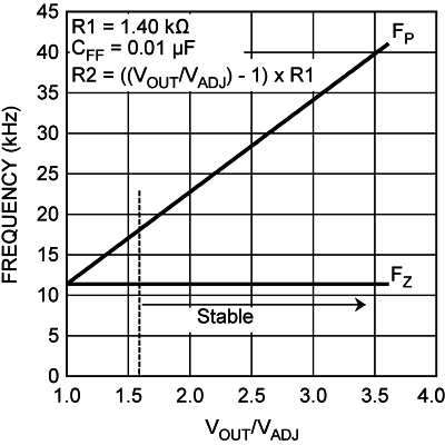 Figure 24. FZERO and FPOLE vs Gain
8.2.2.2 Power Dissipation and Heat Sinking
Additional copper area for heat sinking may be required depending on the maximum device dissipation (PD) and the maximum anticipated ambient temperature (TA) for the device. Under all possible conditions, the junction temperature must be within the range specified under operating conditions.
The total power dissipation of the device is the sum of three different points of dissipation in the device.
The first part is the power that is dissipated in the NMOS pass element, and can be determined with Equation 8:
The second part is the power that is dissipated in the bias and control circuitry and can be determined with Equation 9:
where
- IGND(BIAS) is the portion of the operating ground current of the device that is related to VBIAS.
The third part is the power that is dissipated in portions of the output stage circuitry and can be determined with Equation 10:
where
- IGND(IN) is the portion of the operating ground current of the device that is related to VIN.
The total power dissipation is then:
The maximum allowable junction temperature rise (ΔTJ) depends on the maximum anticipated ambient temperature (TA) for the application, and the maximum allowable operating junction temperature (TJ(MAX)) .
The maximum allowable value for junction-to-ambient thermal resistance, RθJA, can be calculated using Equation 13:
8.2.3 Application Curves
