SNVS482F January 2007 – December 2015
PRODUCTION DATA.
- 1 Features
- 2 Applications
- 3 Description
- 4 Revision History
- 5 Pin Configuration and Functions
- 6 Specifications
- 7 Detailed Description
- 8 Application and Implementation
- 9 Power Supply Recommendations
- 10Layout
- 11Device and Documentation Support
- 12Mechanical, Packaging, and Orderable Information
Package Options
Mechanical Data (Package|Pins)
Thermal pad, mechanical data (Package|Pins)
Orderable Information
6 Specifications
6.1 Absolute Maximum Ratings
over operating free-air temperature range (unless otherwise noted)(1)(2)| MIN | MAX | UNIT | ||
|---|---|---|---|---|
| VIN supply voltage (survival) | −0.3 | 6 | V | |
| VBIAS supply voltage (survival) | −0.3 | 6 | V | |
| VSS soft-start voltage (survival) | −0.3 | 6 | V | |
| VOUT voltage (survival) | −0.3 | 6 | V | |
| IOUT current (survival) | Internally Limited | |||
| Junction temperature | −40 | 150 | °C | |
| Power dissipation(3) | Internally Limited | |||
| Storage temperature, Tstg | −65 | 150 | °C | |
(1) Stresses beyond those listed under Absolute Maximum Ratings may cause permanent damage to the device. These are stress ratings only, which do not imply functional operation of the device at these or any other conditions beyond those indicated under Recommended Operating Conditions. Exposure to absolute-maximum-rated conditions for extended periods may affect device reliability.
(2) If Military/Aerospace specified devices are required, contact the TI Sales Office/ Distributors for availability and specifications.
(3) Device power dissipation must be de-rated based on device power dissipation (PD), ambient temperature (TA), and package junction to ambient thermal resistance (RθJA). Additional heat-sinking may be required to ensure that the device junction temperature (TJ) does not exceed the maximum operating rating. See the Application and Implementation section for details.
6.2 ESD Ratings
| VALUE | UNIT | |||
|---|---|---|---|---|
| V(ESD) | Electrostatic discharge | Human-body model (HBM), per ANSI/ESDA/JEDEC JS-001(1) | ±2000 | V |
(1) JEDEC document JEP155 states that 500-V HBM allows safe manufacturing with a standard ESD control process.
6.3 Recommended Operating Conditions
over operating free-air temperature range (unless otherwise noted)| MIN | NOM | MAX | UNIT | ||
|---|---|---|---|---|---|
| VIN supply voltage (survival) | (VOUT + VDO) to VBIAS | V | |||
| VBIAS supply voltage (survival)(1) | 0.8 V ≤ VOUT ≤ 1.2 V | 3 | 5.5 | V | |
| 1.2 V < VOUT ≤ 1.8 V | 4.5 | 5.5 | V | ||
| VEN voltage | 0 | VBIAS | V | ||
| IOUT | 0 | 3 | mA | ||
| Junction temperature(2) | −40 | 125 | °C | ||
(1) VIN cannot exceed either VBIAS or 4.5 V, whichever value is lower.
(2) Device power dissipation must be de-rated based on device power dissipation (PD), ambient temperature (TA), and package junction-to-ambient thermal resistance (RθJA). Additional heat sinking may be required to ensure that the device junction temperature (TJ) does not exceed the maximum operating rating. See the Application and Implementation section for details.
6.4 Thermal Information
| THERMAL METRIC(1) | LP38852-ADJ | UNIT | |||
|---|---|---|---|---|---|
| KTW (DDPAK/TO-263) | NDZ (TO-220) | DDA (SO PowerPAD) | |||
| 7 PINS | 7 PINS | 8 PINS | |||
| RθJA | Junction-to-ambient thermal resistance | 34.3 | 34.0 | 48.4 | °C/W |
| RθJC(top) | Junction-to-case (top) thermal resistance | 37.6 | 36.4 | 54.6 | °C/W |
| RθJB | Junction-to-board thermal resistance | 25.3 | 25.0 | 29.1 | °C/W |
| ψJT | Junction-to-top characterization parameter | 6.6 | 6.3 | 9.6 | °C/W |
| ψJB | Junction-to-board characterization parameter | 24.0 | 23.6 | 29.0 | °C/W |
| RθJC(bot) | Junction-to-case (bottom) thermal resistance | n/a | n/a | 4.3 | °C/W |
(1) For more information about traditional and new thermal metrics, see the Semiconductor and IC Package Thermal Metrics application report, SPRA953.
6.5 Electrical Characteristics
Unless otherwise specified: VOUT = 0.8 V, VIN = VOUT(NOM) + 1 V, VBIAS = 3 V, VEN = VBIAS, IOUT = 10 mA, CIN = COUT = 10 µF, CBIAS = 1 µF, CSS = open; typical (TYP) limits are for TJ = 25°C only, and minimum (MIN) and maximum (MAX) limits apply over the junction temperature (TJ) range of –40°C to +125°C. Minimum and maximum limits are specified through test, design, or statistical correlation. Typical values represent the most likely parametric norm at TJ = 25°C, and are provided for reference purposes only.| PARAMETER | TEST CONDITIONS | MIN | TYP | MAX | UNIT | |
|---|---|---|---|---|---|---|
| VADJ | VADJ accuracy | VOUT(NOM)+1 V ≤ VIN ≤ VBIAS ≤ 4.5 V(1)
3 V ≤ VBIAS ≤ 5.5 V, 10 mA ≤ IOUT ≤ 1.5 A TJ = 25°C |
492.5 | 500. | 507.5 | mV |
| VOUT(NOM)+1 V ≤ VIN ≤ VBIAS ≤ 4.5 V(1)
3 V ≤ VBIAS ≤ 5.5 V, 10 mA ≤ IOUT ≤ 1.5 A |
485 | 515 | ||||
| VOUT(NOM)+1 V ≤ VIN ≤ VBIAS ≤ 4.5 V(1)
3 V ≤ VBIAS ≤ 5.5 V, 10 mA ≤ IOUT ≤ 1.5 A, 0°C ≤ TJ ≤ +125°C |
490 | 500. | 510 | |||
| VOUT | VOUT range | 3 V ≤ VBIAS ≤ 5.5 V | 0.8 | 1.2 | V | |
| 4.5 V ≤ VBIAS ≤ 5.5 V | 0.8 | 1.8 | ||||
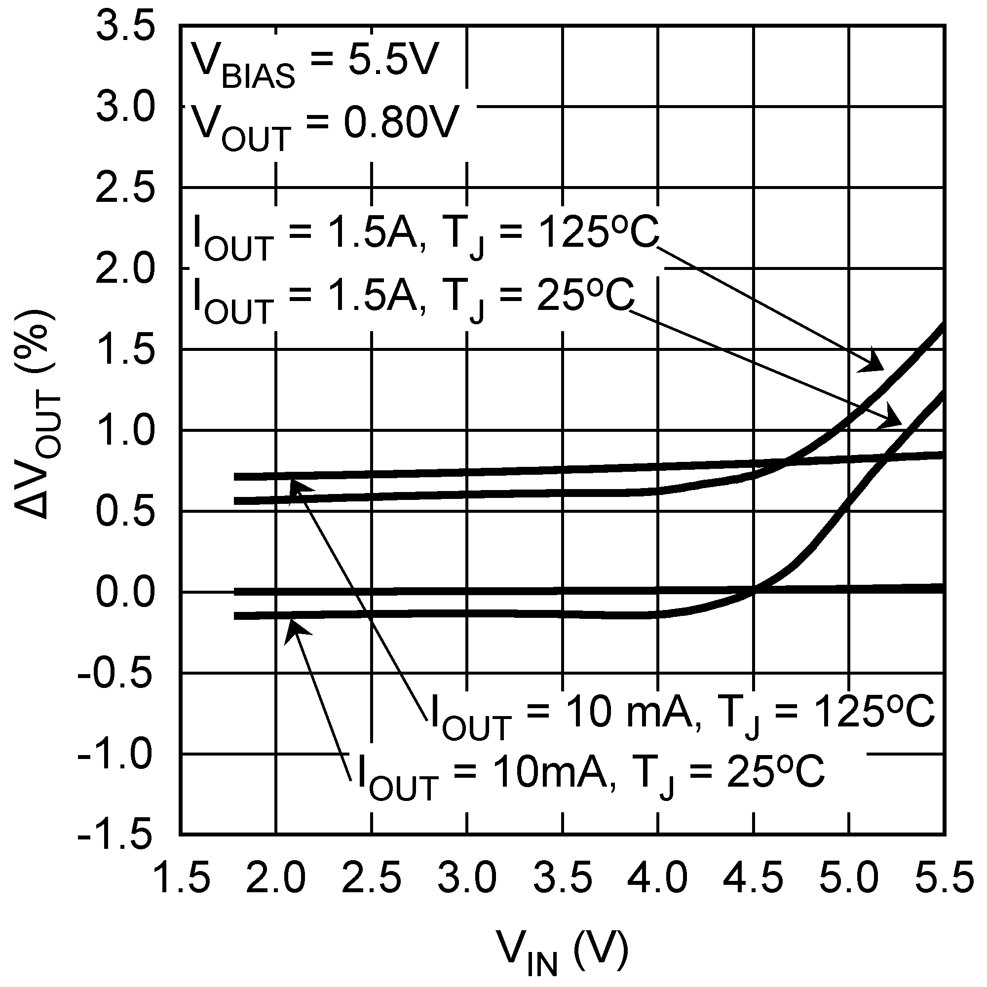
| ΔVOUT/ΔVIN | Line regulation, VIN(2) | VOUT(NOM)+1 V ≤ VIN ≤ VBIAS | 0.04 | %/V | ||
| ΔVOUT/ΔVBIAS | Line regulation, VBIAS(2) | 3 V ≤ VBIAS ≤ 5.5 V | 0.1 | %/V | ||
| ΔVOUT/ΔIOUT | Output voltage load regulation(3) | 10 mA ≤ IOUT ≤ 1.5 A | 0.2 | %/A | ||
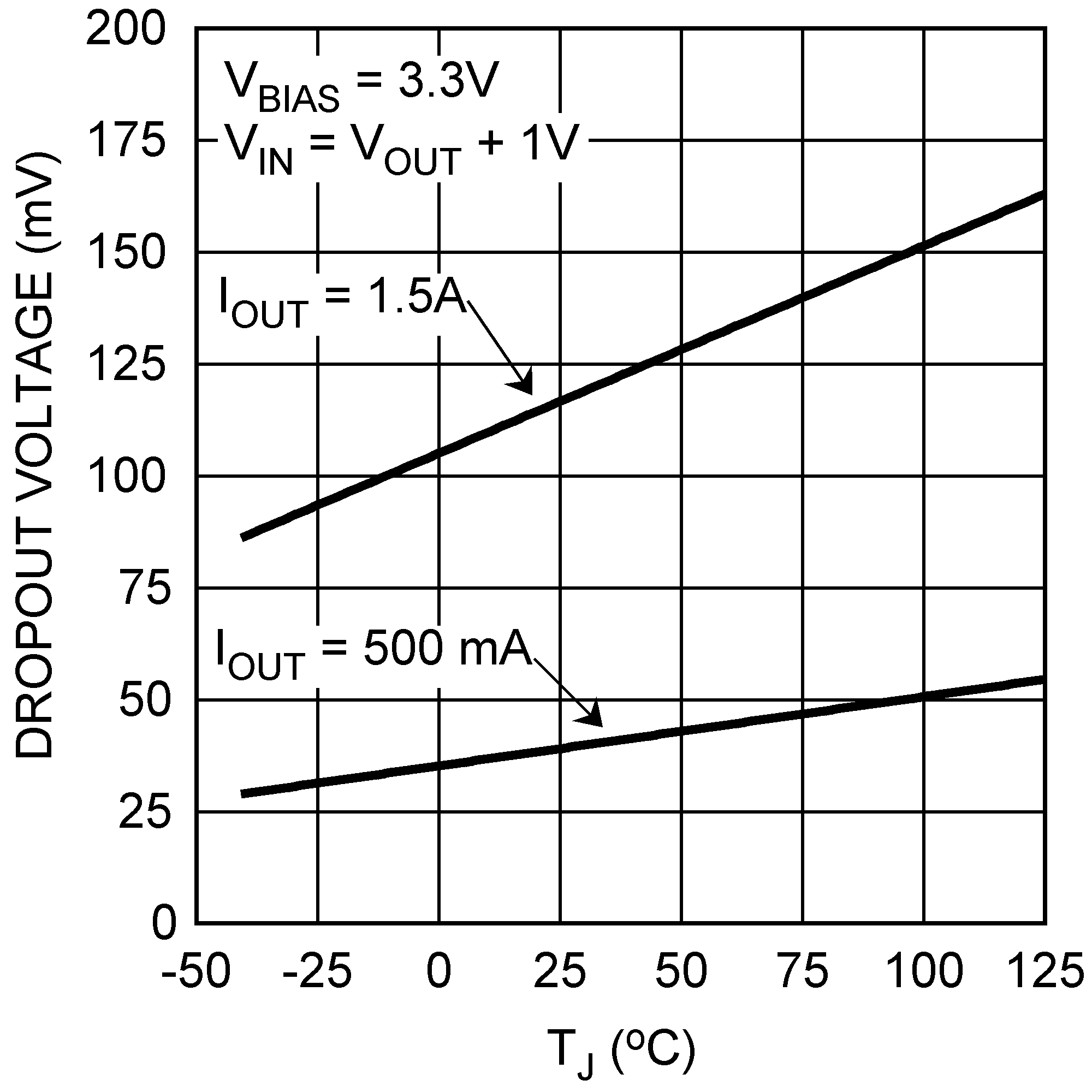
| VDO | Dropout voltage(4) | IOUT = 1.5 A, TJ = 25°C | 130 | 165 | mV | |
| IOUT = 1.5 A | 180 | |||||
| IGND(IN) | Quiescent current drawn from VIN supply | VOUT = 0.8 V, VBIAS = 3 V 10 mA ≤ IOUT ≤ 1.5 A TJ = 25°C |
7 | 8.5 | mA | |
| VOUT = 0.8 V, VBIAS = 3 V 10 mA ≤ IOUT ≤ 1.5 A |
9 | |||||
| VEN ≤ 0.5 V, TJ = 25°C | 1 | 100 | μA | |||
| VEN ≤ 0.5 V | 300 | |||||
| IGND(BIAS) | Quiescent current drawn from VBIAS supply | 10 mA ≤ IOUT ≤ 1.5 A, TJ = 25°C | 3 | 3.8 | mA | |
| 10 mA ≤ IOUT ≤ 1.5 A | 4.5 | |||||
| VEN ≤ 0.5 V, TJ = 25°C | 100 | 170 | μA | |||
| VEN ≤ 0.5 V | 200 | |||||
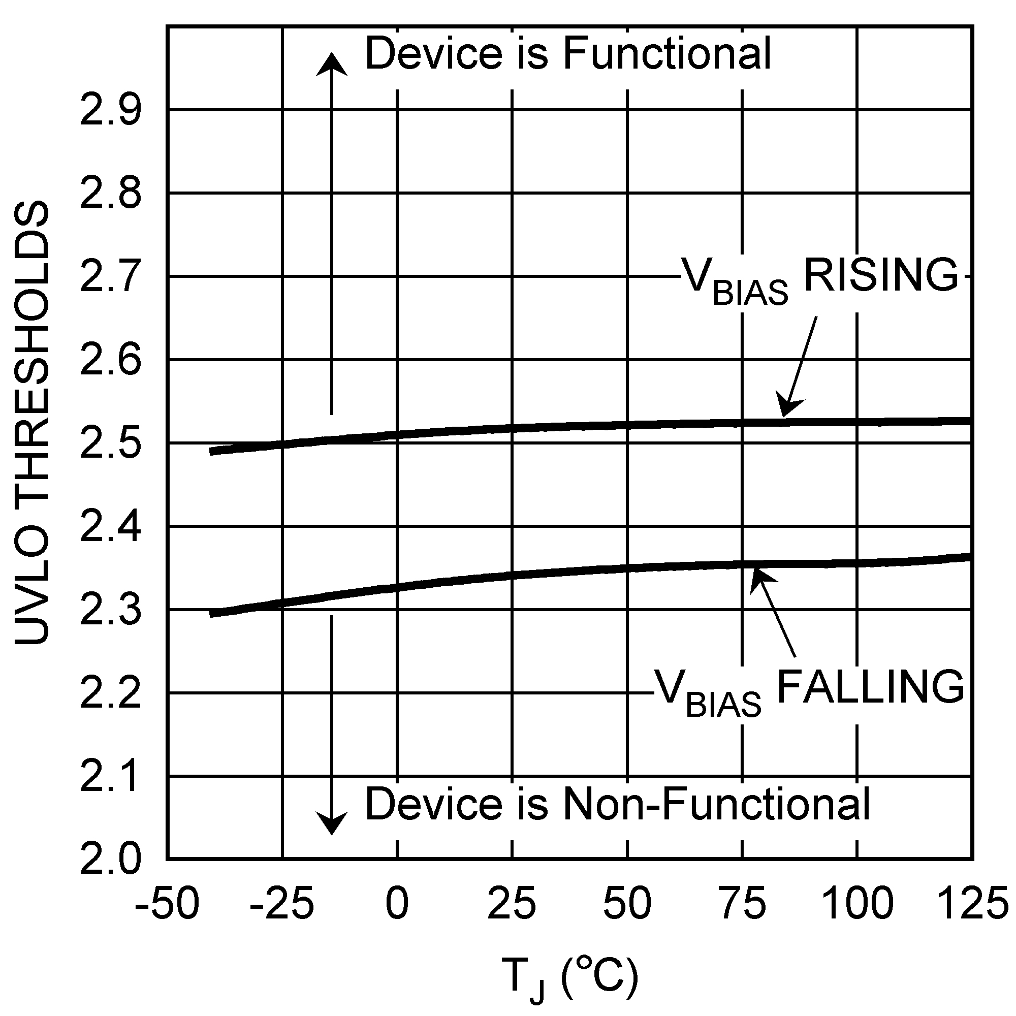
| UVLO | Undervoltage lockout threshold | VBIAS rising until device is functional TJ = 25°C |
2.2 | 2.45 | 2.7 | V |
| VBIAS rising until device is functional | 2 | 2.9 | ||||
| UVLO(HYS) | Undervoltage lockout hysteresis | VBIAS falling from UVLO threshold until device is non-functional TJ = 25°C |
60 | 150 | 300 | mV |
| VBIAS falling from UVLO threshold until device is non-functional | 50 | 350 | ||||
| ISC | Output short-circuit current | VIN = VOUT(NOM) + 1 V, VBIAS = 3 V, VOUT = 0 V |
4.5 | A | ||
| SOFT-START | ||||||
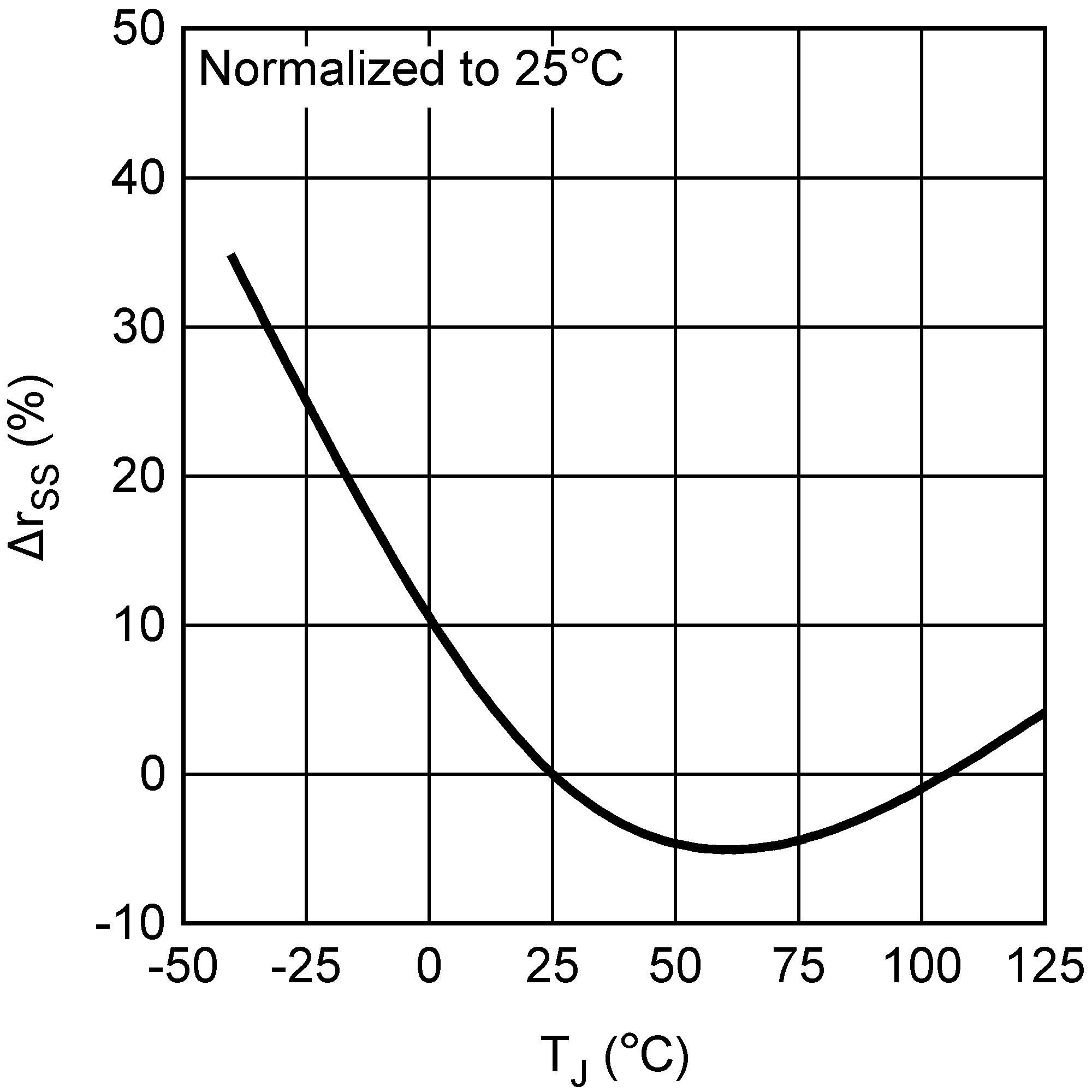
| rSS | Soft-start internal resistance | 11 | 13.5 | 16 | kΩ | |
| tSS | Soft-start time tSS = CSS × rSS × 5 |
CSS = 10 nF | 675 | μs | ||
| ENABLE | ||||||
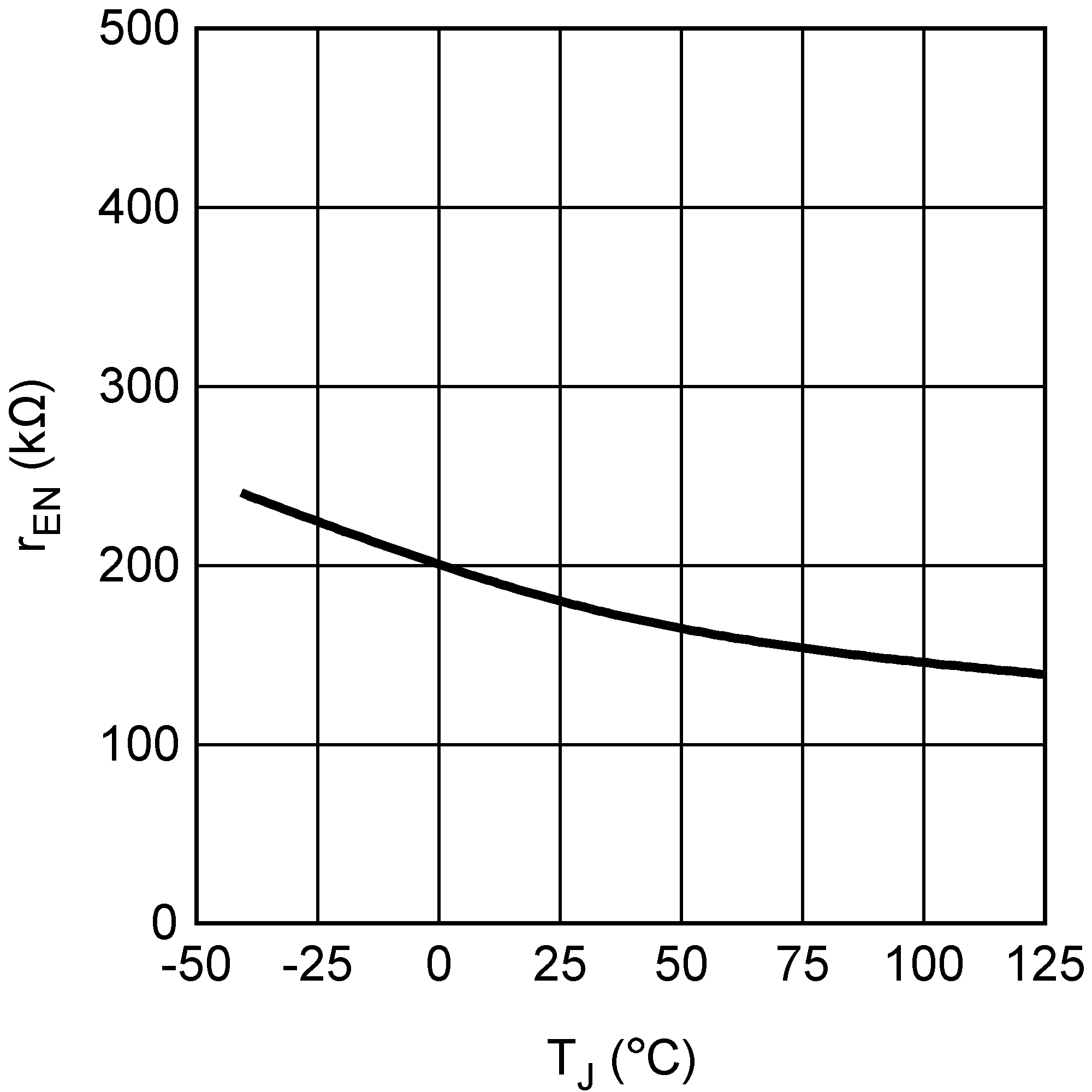
| IEN | ENABLE pin current | VEN = VBIAS | 0.01 | μA | ||
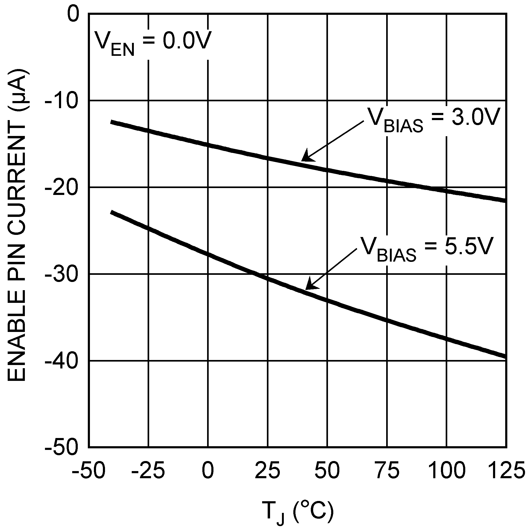
| VEN = 0 V, VBIAS = 5.5 V, TJ = 25°C | –19 | –30 | –40 | |||
| VEN = 0 V, VBIAS = 5.5 V | –13 | –51 | ||||
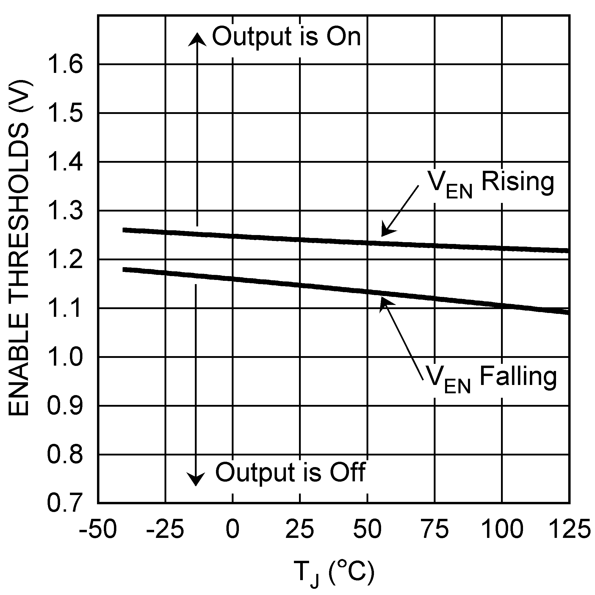
| VEN(ON) | Enable voltage threshold | VEN rising until output = ON, TJ = 25°C | 1 | 1.25 | 1.5 | V |
| VEN rising until output = ON | 0.9 | 1.55 | ||||
| VEN(HYS) | Enable voltage hysteresis | VEN falling from VEN(ON) until Output = OFF TJ = 25°C |
50 | 100 | 150 | mV |
| VEN falling from VEN(ON) until Output = OFF | 30 | 200 | ||||
| AC PARAMETERS | ||||||
| PSRR (VIN) | Ripple rejection for VIN input voltage | VIN = VOUT(NOM) + 1 V, ƒ = 120 Hz |
80 | dB | ||
| VIN = VOUT(NOM) + 1 V, ƒ = 1 kHz |
65 | |||||
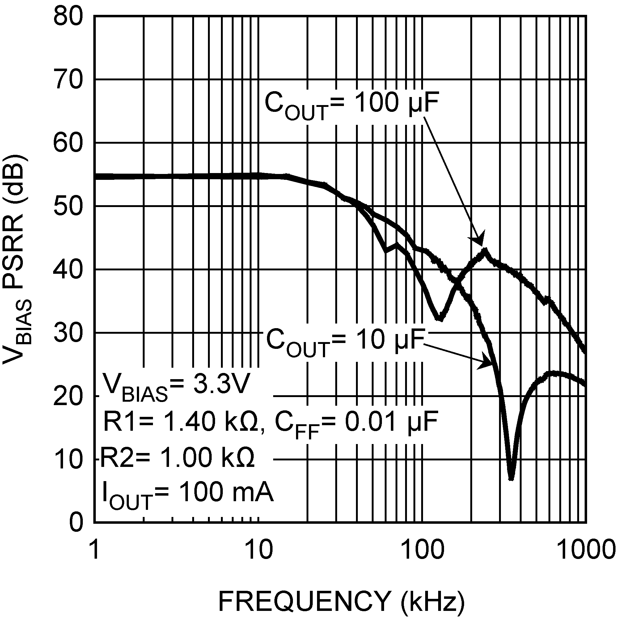
| PSRR (VBIAS) | Ripple rejection for VBIAS voltage | VBIAS = VOUT(NOM) + 3 V, ƒ= 120 Hz |
58 | dB | ||
| VBIAS = VOUT(NOM) + 3 V, ƒ = 1 kHz |
58 | |||||
| en | Output noise density | ƒ = 120 Hz | 1 | µV/√Hz | ||
| Output noise voltage | BW = 10 Hz − 100 kHz | 150 | µVRMS | |||
| BW = 300 Hz − 300 kHz | 90 | |||||
| THERMAL PARAMETERS | ||||||
| TSD | Thermal shutdown junction temperature | 160 | °C | |||
| TSD(HYS) | Thermal shutdown hysteresis | 10 | °C | |||
(1) VIN cannot exceed either VBIAS or 4.5 V, whichever value is lower.
(2) Output voltage line regulation is defined as the change in output voltage from nominal value resulting from a change in input voltage.
(3) Output voltage load regulation is defined as the change in output voltage from nominal value as the load current increases from no load to full load.
(4) Dropout voltage is defined as the input to output voltage differential (VIN – VOUT) where the input voltage is low enough to cause the output voltage to drop 2% from the nominal value.
6.6 Timing Requirements
| MIN | NOM | MAX | UNIT | ||
|---|---|---|---|---|---|
| tOFF | Turnoff delay time, RLOAD x COUT << tOFF | 20 | µs | ||
| tON | Turnon delay time, RLOAD x COUT << tON | 15 | µs | ||
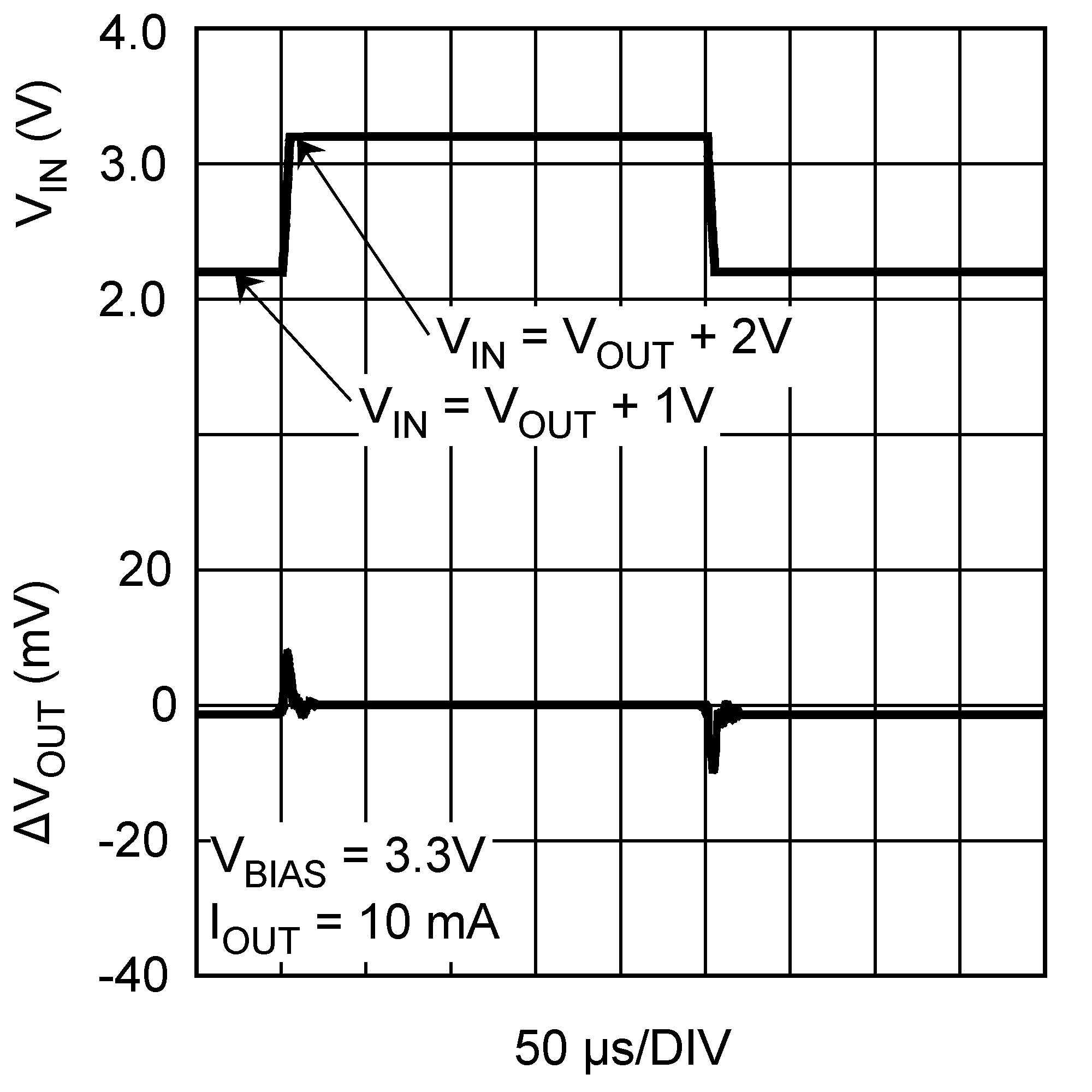
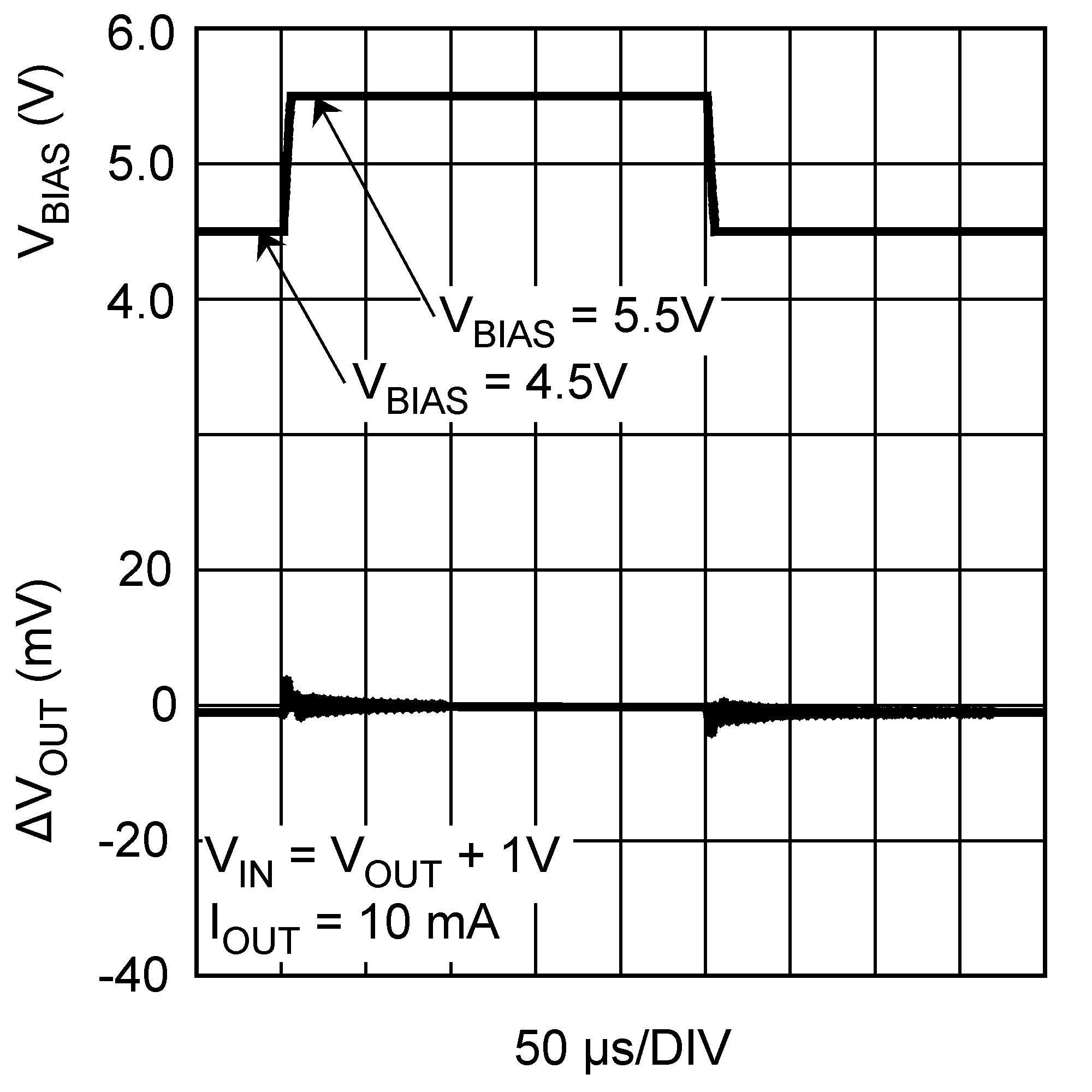
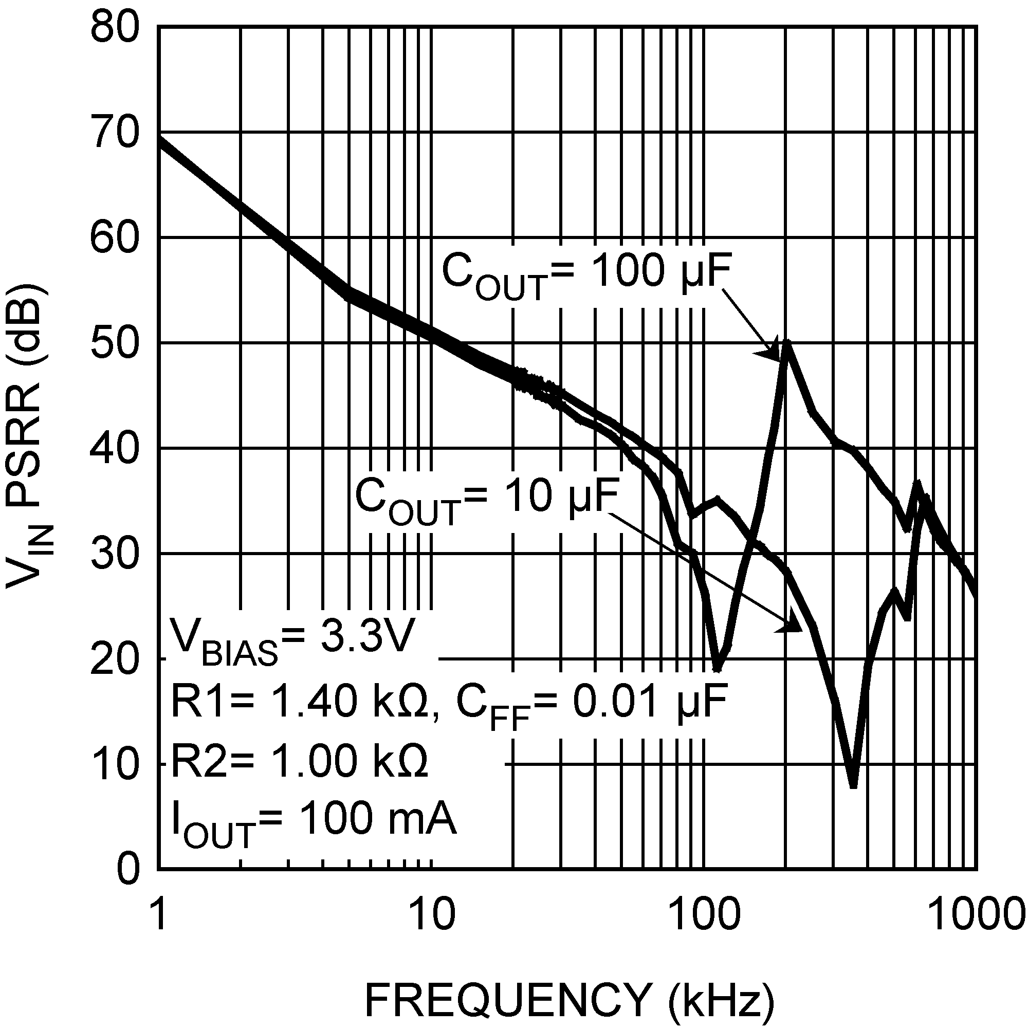
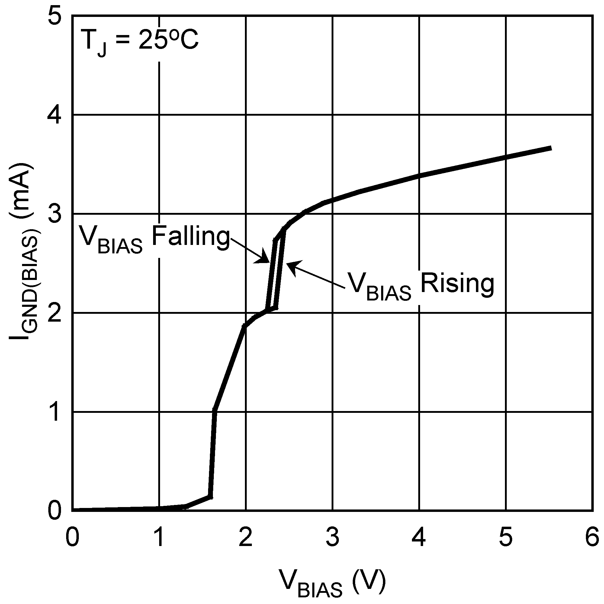
6.7 Typical Characteristics
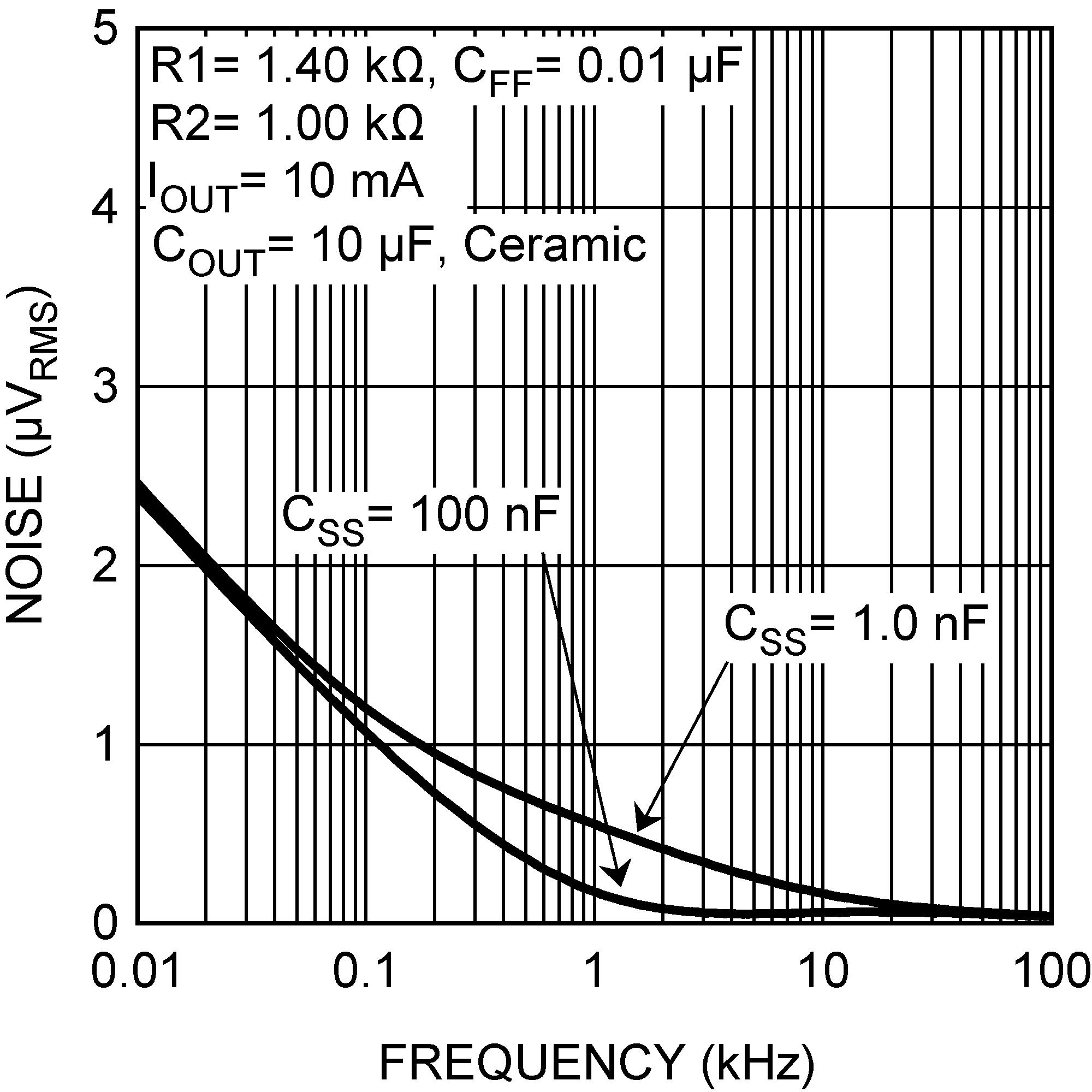
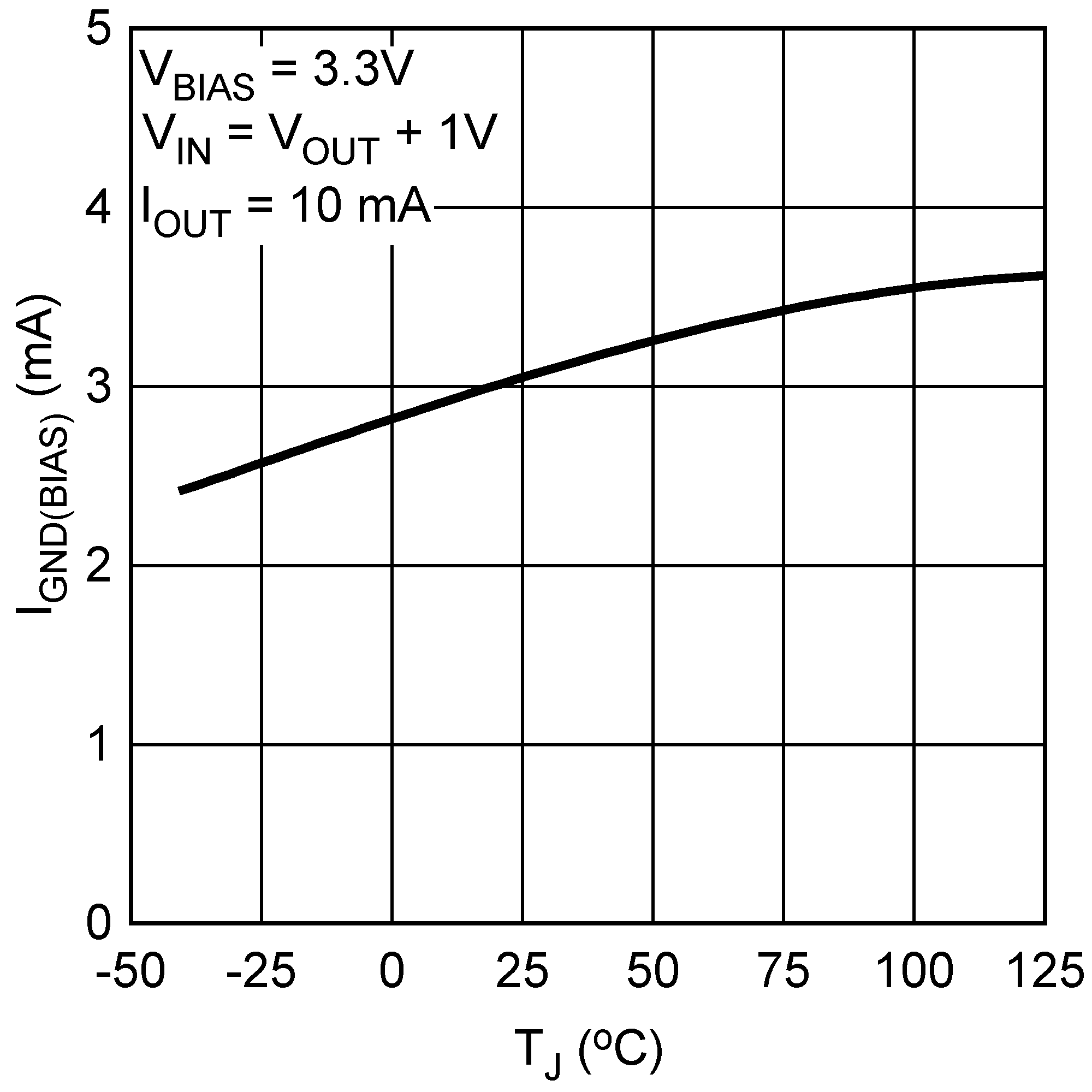
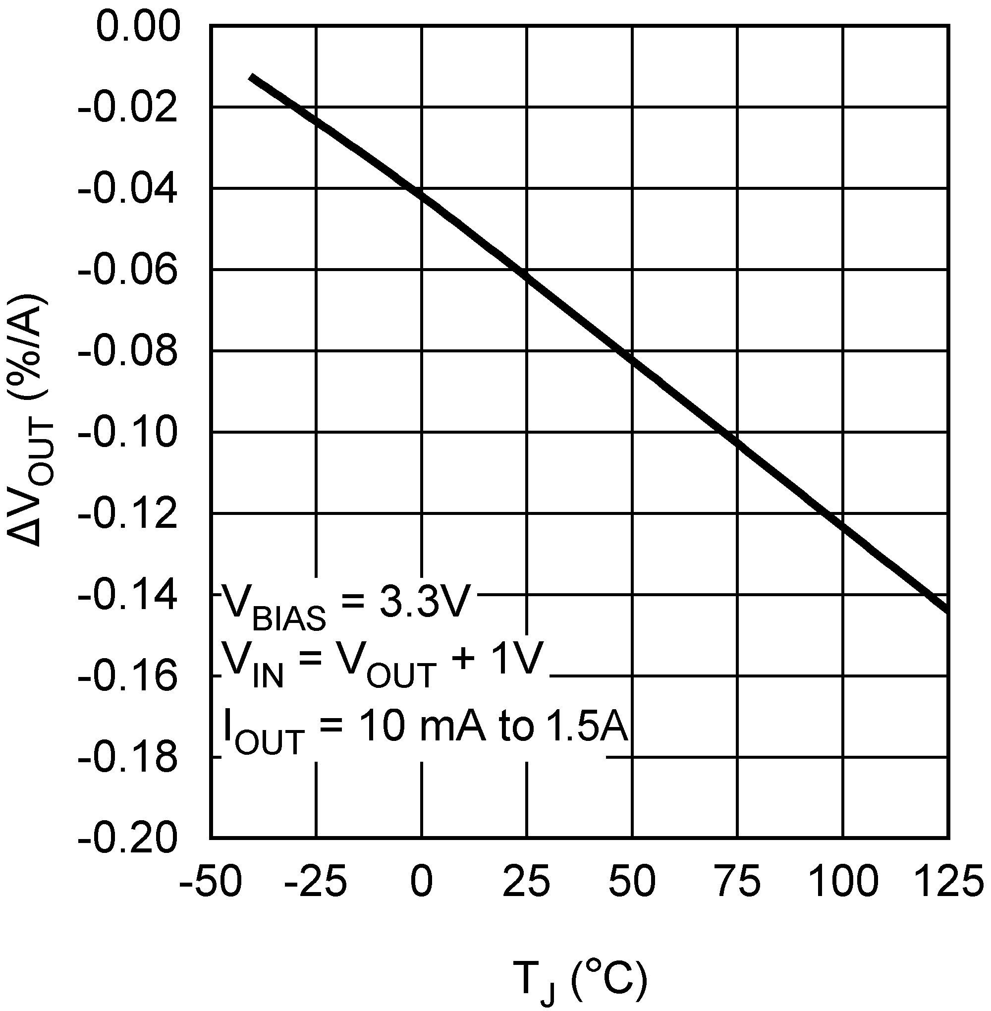
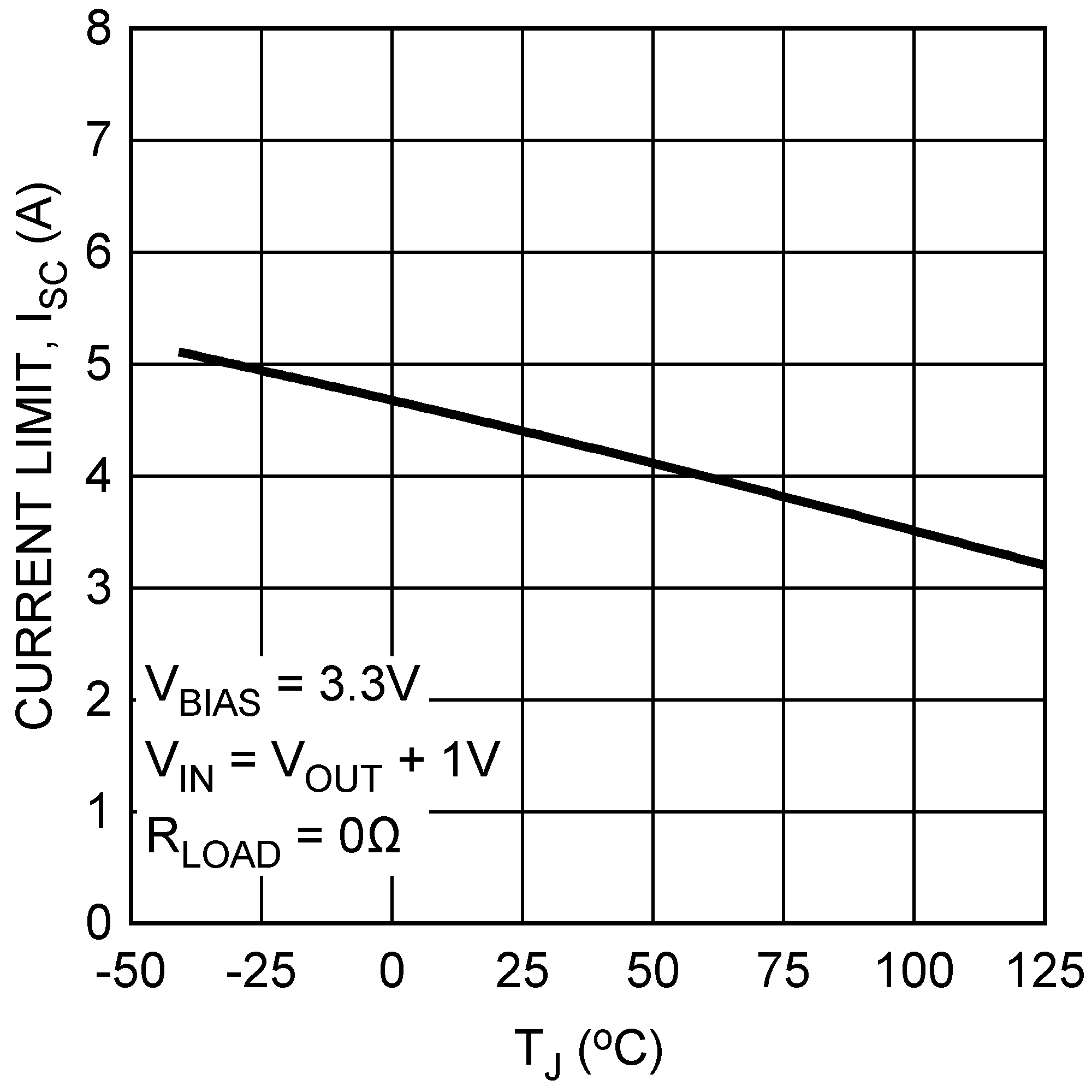
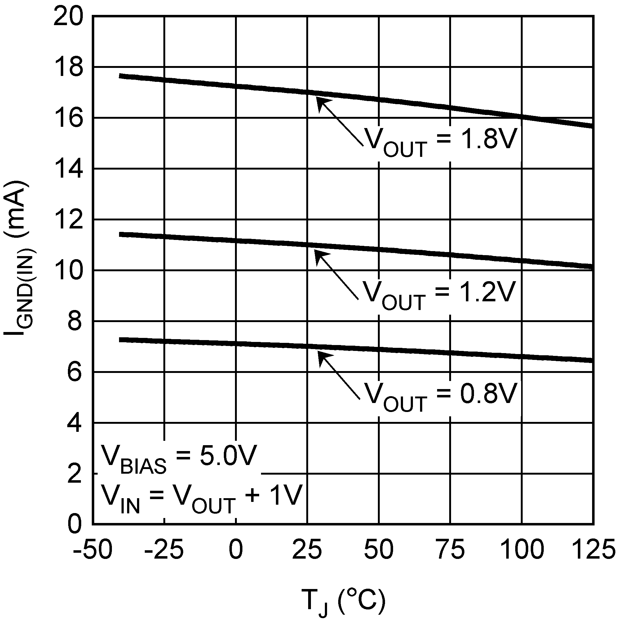
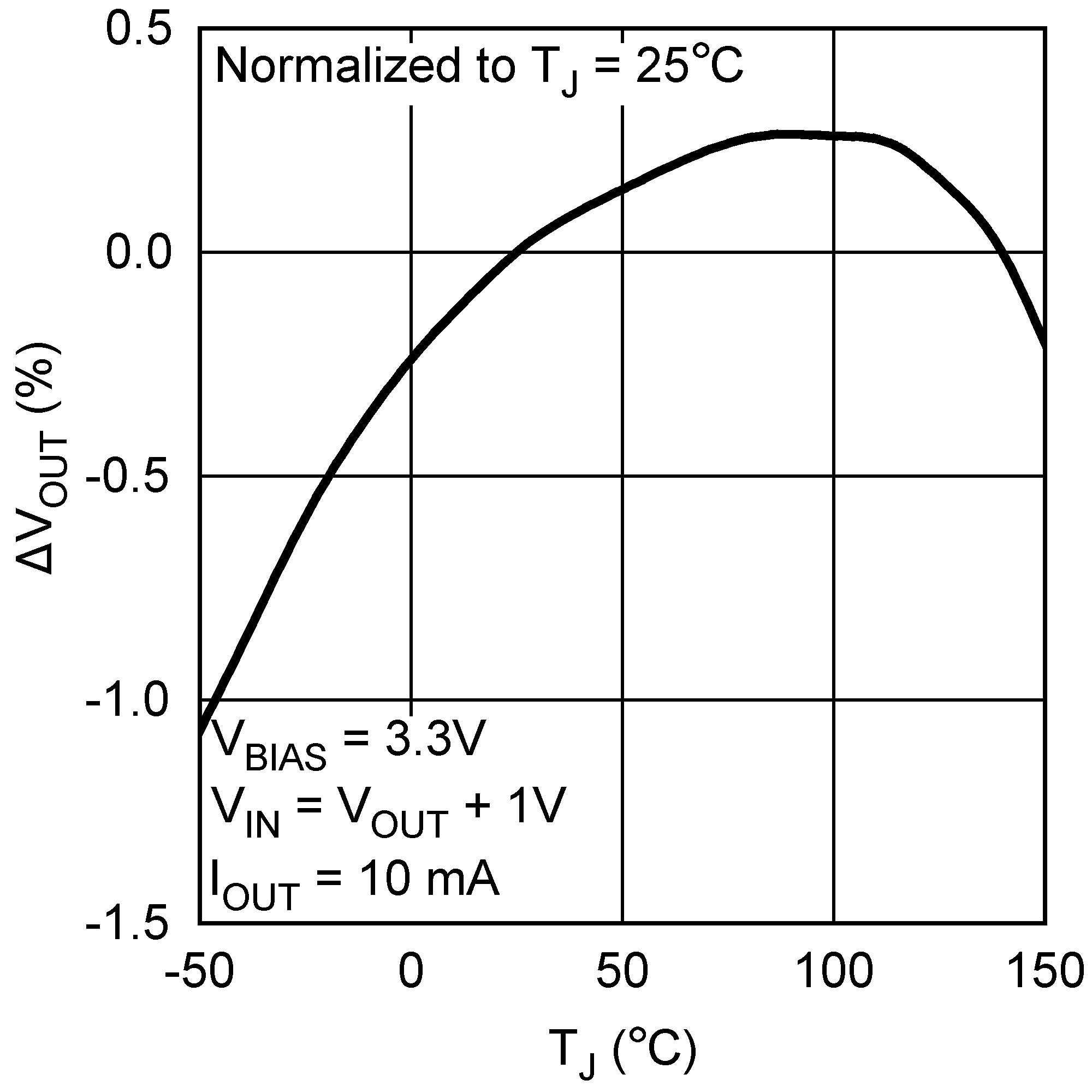
Refer to the Typical Application Circuit. Unless otherwise specified: TJ = 25°C, R1 = 1.4 kΩ, R2 = 1 kΩ, CFF= 0.01 µF,VIN = VOUT(NOM) + 1 V, VBIAS = 3 V, IOUT = 10 mA, CIN = 10-µF ceramic, COUT = 10-µF ceramic, CBIAS = 1-µF Ceramic, CSS = open.
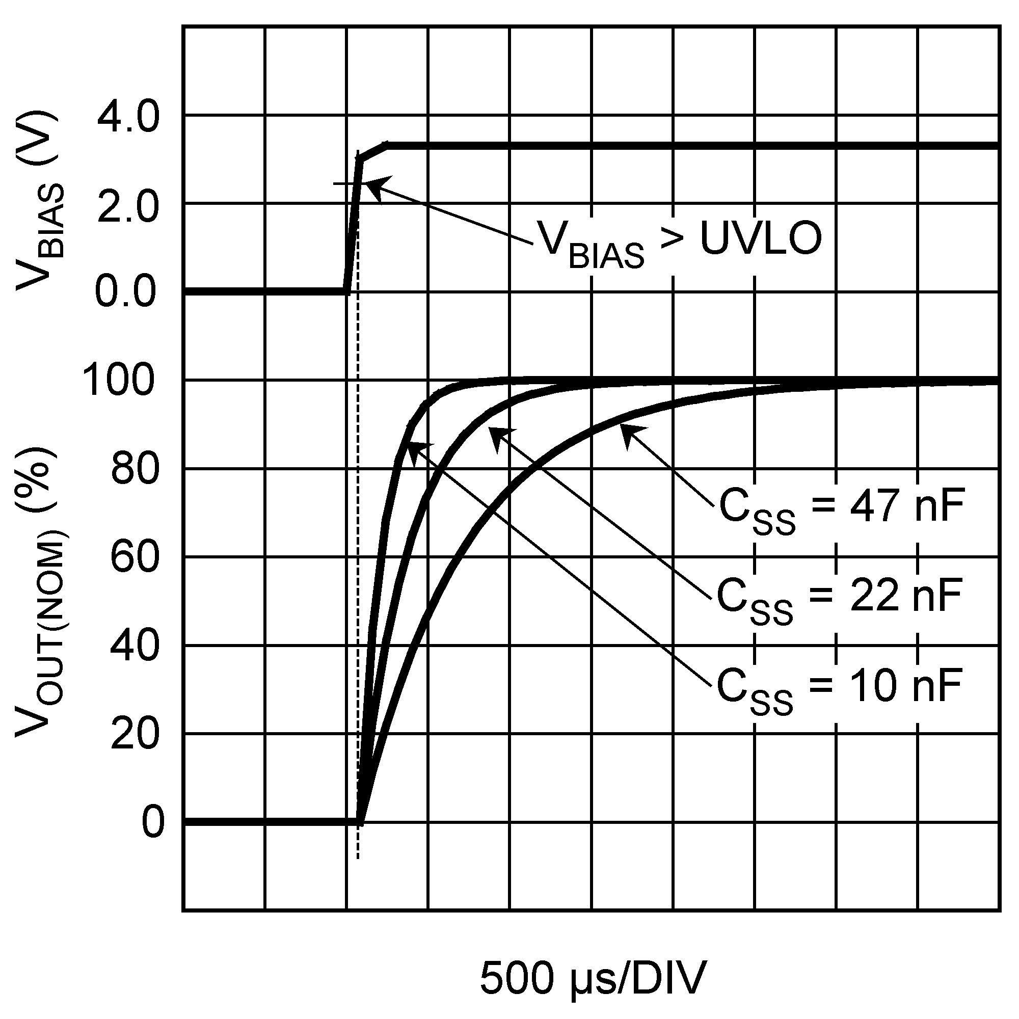
| 10 nF To 47 nF |
