SNVS336F June 2006 – August 2015 LP38856
PRODUCTION DATA.
- 1 Features
- 2 Applications
- 3 Description
- 4 Revision History
- 5 Pin Configuration and Functions
- 6 Specifications
- 7 Detailed Description
- 8 Application and Implementation
- 9 Power Supply Recommendations
- 10Layout
- 11Device and Documentation Support
- 12Mechanical, Packaging, and Orderable Information
Package Options
Mechanical Data (Package|Pins)
Thermal pad, mechanical data (Package|Pins)
- KTT|5
Orderable Information
1 Features
- Input Voltage: 1.1 V to 5.5 V
- Wide VBIAS Supply Operating Range: 3 V to 5.5 V
- Standard VOUT: 0.8 V and 1.2 V
- Stable with 10-µF Ceramic Capacitors
- Dropout Voltage of 240 mV (Typical) at 3-A Load Current
- Precision Output Voltage Across All Line and Load Conditions:
- ±1% for TJ = 25°C
- ±2% for 0°C ≤ TJ ≤ +125°C
- ±3% for –40°C ≤ TJ ≤ +125°C
- Overtemperature and Overcurrent Protection
- –40°C to +125°C Operating Temperature Range
2 Applications
- ASIC Power Supplies In:
- Desktops, Notebooks, and Graphics Cards, Servers
- Gaming Set Top Boxes, Printers and Copiers
- Server Core and I/O Supplies
- DSP and FPGA Power Supplies
- SMPS Post-Regulator
3 Description
The LP38856 is a high-current, fast-response regulator which can maintain output voltage regulation with an extremely low input-to-output voltage drop. Fabricated on a CMOS process, the device operates from two input voltages: VBIAS provides power for the internal bias and control circuits, as well as drive for the gate of the N-MOS power transistor, while VIN supplies power to the load. The use of an external bias rail allows the part to operate from ultra-low VIN voltages. Unlike bipolar regulators, the CMOS architecture consumes extremely low quiescent current at any output load current. The use of an N-MOS power transistor results in wide bandwidth, yet minimum external capacitance is required to maintain loop stability.
The fast transient response of this device makes it suitable for use in powering DSP, microcontroller core voltages, and switch mode power supply post regulators. The LP38856 is available in 5-pin TO-220 and DDPAK/TO-263 packages.
- Dropout Voltage: 240 mV (typical) at 3-A load current.
- Low Ground Pin Current: 10 mA (typical) at 3-A load current.
- Shutdown Current: 1 µA (typical) IIN(GND) when EN pin is low.
- Precision Output Voltage: ±1% for TJ = 25°C and ±2% for 0°C ≤ TJ ≤ +125°C, across all line and load conditions.
Device Information(1)
| PART NUMBER | PACKAGE | BODY SIZE (NOM) |
|---|---|---|
| LP38856 | DDPAK/TO-263 (5) | 10.16 mm × 8.42 mm |
| TO-220 (5) | 14.986 mm × 10.16 mm |
- For all available packages, see the orderable addendum at the end of the data sheet.
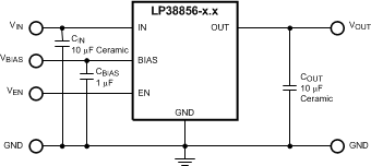
Typical Application Circuit
