SNVS256D Novmeber 2003 – November 2016 LP3943
PRODUCTION DATA.
- 1 Features
- 2 Applications
- 3 Description
- 4 Revision History
- 5 Pin Configuration and Functions
- 6 Specifications
- 7 Detailed Description
- 8 Application and Implementation
- 9 Power Supply Recommendations
- 10Layout
- 11Device and Documentation Support
- 12Mechanical, Packaging, and Orderable Information
Package Options
Mechanical Data (Package|Pins)
- RTW|24
Thermal pad, mechanical data (Package|Pins)
Orderable Information
1 Features
2 Applications
- Customized Flashing LED Lights for Cellular Phones
- Portable Applications
- Digital Cameras
- Indicator Lamps
- General Purpose I/O Expander
- Toys
3 Description
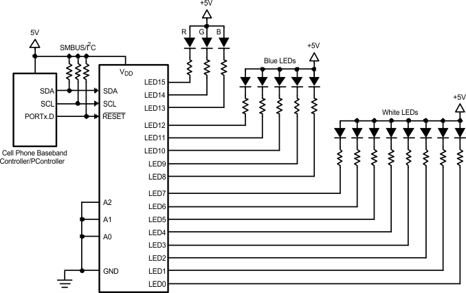
The LP3943 is an integrated device capable of independently driving 16 LEDs. This device also contains an internal precision oscillator that provides all the necessary timing required for driving each LED. Two prescaler registers, along with two PWM registers, provide a versatile duty-cycle control. The LP3943 contains the ability to dim LEDs in SMBUS/I2C applications where it is required, to cut down on bus traffic.
Traditionally, dimming LEDs using a serial shift register such as 74LS594/5 requires a large amount of traffic on the serial bus. The LP3943 instead requires only the setup of the frequency and duty cycle for each output pin; from then on, only a single command from the host is required to turn each individual open drain output to an ON or OFF state, or to cycle a programmed frequency and duty cycle. Maximum output sink current is 25 mA per pin and 200 mA per package. Any ports not used for controlling the LEDs can be used for general purpose input/output expansion.
Device Information(1)
| PART NUMBER | PACKAGE | BODY SIZE (NOM) |
|---|---|---|
| LP3943 | WQFN (24) | 4.00 mm × 4.00 mm |
- For all available packages, see the orderable addendum at the end of the data sheet.
Typical Application Circuit
