SNVS179F February 2003 – September 2015 LP3995
PRODUCTION DATA.
- 1 Features
- 2 Applications
- 3 Description
- 4 Revision History
- 5 Pin Configuration and Functions
- 6 Specifications
- 7 Parameter Measurement Information
- 8 Detailed Description
- 9 Application and Implementation
- 10Power Supply Recommendations
- 11Layout
- 12Device and Documentation Support
- 13Mechanical, Packaging, and Orderable Information
Package Options
Mechanical Data (Package|Pins)
Thermal pad, mechanical data (Package|Pins)
Orderable Information
1 Features
- Input Range: 2.5 V to 6 V
- Accurate Output Voltage: ±75 mV / 2%
- Typical Dropout with 150 mA Load: 60 mV
- Virtually Zero Quiescent Current When Disabled
- Low Output Voltage Noise
- Stable With a 1-µF Output Capacitor
- Output Current: 150 mA
- Fast Turnon: 30 µs (Typical)
- Fast Turnoff: 175 µs (Typical)
- Stable With Ceramic Capacitor
- Logic Controlled Enable
- Fast Turnon
- Active Disable for Fast Turnoff
- Thermal-Overload and Short-Circuit Protection
- −40 to +125°C Junction Temperature Range for Operation
2 Applications
- GSM Portable Phones
- CDMA Cellular Handsets
- Wideband CDMA Cellular Handsets
- Bluetooth Devices
- Portable Information Appliances
3 Description
The LP3995 linear regulator is designed to meet the requirements of portable battery-powered applications, providing an accurate output voltage with low noise and low quiescent current. Ideally suited for powering RF and analog devices, this device can also be used to meet more general circuit needs in which a fast turnoff is essential.
For battery-powered applications the low dropout and low ground current provided by the device allows the lifetime of the battery to be maximized. The Enable(/Disable) control function allows the system to further extend the battery lifetime by reducing the power consumption to virtually zero. This function also incorporates an active discharge circuit on the output for faster device shutdown. Where the fast turnoff is not required the LP3999 linear regulator is recommended. The LP3995 also features internal protection against short-circuit currents and overtemperature conditions.
The LP3995 is designed to be stable with small 1-µF ceramic capacitors. The small outline of the LP3995 DSBGA package with the required ceramic capacitors can realize a system application within minimal board area. Performance is specified for a −40°C to +125°C temperature range.
The LP3995 is available in fixed output voltages from 1.5 V to 3.3 V, in DSBGA or WSON packages. For other package options or output-voltage options, contact your local TI sales office.
Device Information(1)
| PART NUMBER | PACKAGE | BODY SIZE |
|---|---|---|
| LP3995 | DSBGA (5) | 1.502 mm × 1.045 mm (MAX) |
| WSON (6) | 3.29 mm × 2.92 mm (NOM) |
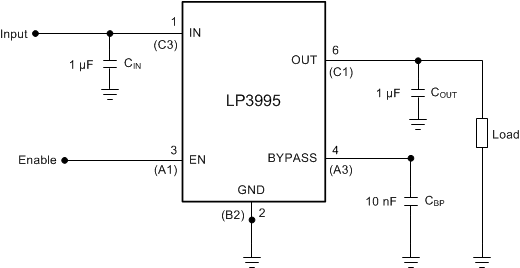
Typical Application Circuit
