SNVS345G June 2006 – December 2014 LP5951
PRODUCTION DATA.
- 1 Features
- 2 Applications
- 3 Description
- 4 Revision History
- 5 Pin Configuration and Functions
- 6 Specifications
- 7 Detailed Description
- 8 Application and Implementation
- 9 Power Supply Recommendations
- 10Layout
- 11Device and Documentation Support
- 12Mechanical, Packaging, and Orderable Information
Package Options
Mechanical Data (Package|Pins)
Thermal pad, mechanical data (Package|Pins)
Orderable Information
7 Detailed Description
7.1 Overview
The LP5951 regulator is designed to meet the requirements of portable battery-powered systems providing a regulated output voltage and low quiescent current. When switched to shutdown mode via a logic signal at the EN pin, the power consumption is reduced to virtually zero.
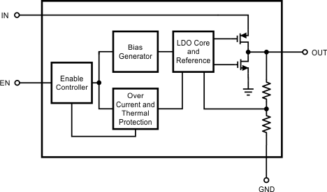
7.2 Functional Block Diagram
7.3 Feature Description
7.3.1 No-Load Stability
The LP5951 will remain stable and in regulation with no external load. This is an important consideration in some circuits, for example CMOS RAM keep-alive applications.
7.3.2 Enable Operation
The LP5951 may be switched ON or OFF by a logic input at the Enable pin, EN. A logic high at this pin will turn the device on. When the EN pin is low, the regulator output is off and the device typically consumes 5 nA.
If the application does not require the enable switching feature, the EN pin should be tied to VIN to keep the regulator output permanently on.
To ensure proper operation, the signal source used to drive the VEN input must be able to swing above and below the specified turn-on/off voltage thresholds listed in the Enable Control Characteristics table, VIL and VIH.
7.3.3 Fast Turn Off And On
The controlled switch-off feature of the device provides a fast turn off by discharging the output capacitor via an internal FET device. This discharge is current limited by the RDSon of this switch.
Fast turnon is ensured by an optimized architecture allowing a very fast ramp of the output voltage to reach the target voltage.
7.3.4 Short-Circuit Protection
The LP5951 is short circuit protected and in the event of a peak over-current condition, the output current through the PMOS will be limited.
If the over-current condition exists for a longer time, the average power dissipation will increase depending on the input to output voltage difference until the thermal shutdown circuitry will turn off the PMOS.
Please refer to the Thermal Information section for power dissipation calculations.
7.3.5 Thermal-Overload Protection
Thermal-Overload Protection limits the total power dissipation in the LP5951. When the junction temperature exceeds TJ = 160°C typ., the shutdown logic is triggered and the PMOS is turned off, allowing the device to cool down. After the junction temperature dropped by 20°C (temperature hysteresis), the PMOS is activated again. This results in a pulsed output voltage during continuous thermal-overload conditions.
The Thermal-Overload Protection is designed to protect the LP5951 in the event of a fault condition. For normal, continuous operation, do not exceed the absolute maximum junction temperature rating of TJ = 150°C (see Absolute Maximum Ratings).
7.3.6 Reverse Current Path
The internal PFET pass device in LP5951 has an inherent parasitic body diode. During normal operation, the input voltage is higher than the output voltage and the parasitic diode is reverse biased. However, if the output is pulled above the input in an application, then current flows from the output to the input as the parasitic diode gets forward biased. The output can be pulled above the input as long as the current in the parasitic diode is limited to 50 mA.
For currents above this limit an external Schottky diode must be connected from VOUT to VIN (cathode on VIN, anode on VOUT).
7.4 Device Functional Modes
7.4.1 Enable (EN)
The EN pin voltage must be higher than the VIH threshold to ensure that the device is fully enabled under all operating conditions. The EN pin voltage must be lower than the VIL threshold to ensure that the device is fully disabled. However if the application does not require the shutdown feature, the VEN pin can be tied to VIN to keep the regulator output permanently on.
7.4.2 Minimum Operating Input Voltage (VIN)
The LP5951 internal circuitry is not fully functional until VIN is at least 1.8 V. The output voltage is not regulated until VIN ≥ (VOUT + VDO), or 1.8 V, whichever is higher.