SNVSB83B June   2019  – January 2020 LP8867-Q1 , LP8869-Q1

PRODUCTION DATA.  

  1. Features
  2. Applications
  3. Description
    1.     Simplified Schematic
    2.     LED Backlight Efficiency
  4. Revision History
  5. Device Comparison Table
  6. Pin Configuration and Functions
    1.     Pin Functions
  7. Specifications
    1. 7.1  Absolute Maximum Ratings
    2. 7.2  ESD Ratings
    3. 7.3  Recommended Operating Conditions
    4. 7.4  Thermal Information
    5. 7.5  Electrical Characteristics
    6. 7.6  Internal LDO Electrical Characteristics
    7. 7.7  Protection Electrical Characteristics
    8. 7.8  Current Sinks Electrical Characteristics
    9. 7.9  PWM Brightness Control Electrical Characteristics
    10. 7.10 Boost and SEPIC Converter Characteristics
    11. 7.11 Logic Interface Characteristics
    12. 7.12 Typical Characteristics
  8. Detailed Description
    1. 8.1 Overview
    2. 8.2 Functional Block Diagram
    3. 8.3 Feature Description
      1. 8.3.1 Integrated DC-DC Converter
        1. 8.3.1.1 DC-DC Converter Parameter Configuration
          1. 8.3.1.1.1 Switching Frequency
          2. 8.3.1.1.2 Spread Spectrum and External SYNC
          3. 8.3.1.1.3 Recommended Component Value and Internal Parameters
          4. 8.3.1.1.4 DC-DC Converter Switching Current Limit
          5. 8.3.1.1.5 DC-DC Converter Light Load Mode
        2. 8.3.1.2 Adaptive Voltage Control
          1. 8.3.1.2.1 Using Two-Divider
          2. 8.3.1.2.2 Using T-Divider
          3. 8.3.1.2.3 Feedback Capacitor
      2. 8.3.2 Internal LDO
      3. 8.3.3 LED Current Sinks
        1. 8.3.3.1 LED Output Configuration
        2. 8.3.3.2 LED Current Setting
        3. 8.3.3.3 Brightness Control
      4. 8.3.4 Power-Line FET Control
      5. 8.3.5 LED Current Dimming With External Temperature Sensor
      6. 8.3.6 Fault Detections and Protection
        1. 8.3.6.1 Supply Fault and Protection
          1. 8.3.6.1.1 VIN Undervoltage Fault (VIN_UVLO)
          2. 8.3.6.1.2 VIN Overvoltage Fault (VIN_OVP)
          3. 8.3.6.1.3 VIN Overcurrent Fault (VIN_OCP)
        2. 8.3.6.2 Boost Fault and Protection
          1. 8.3.6.2.1 Boost Overvoltage Fault (BST_OVP)
          2. 8.3.6.2.2 SW Overvoltage Fault (SW_OVP)
        3. 8.3.6.3 LED Fault and Protection (LED_OPEN and LED_SHORT)
        4. 8.3.6.4 Thermal Fault and Protection (TSD)
        5. 8.3.6.5 Overview of the Fault and Protection Schemes
    4. 8.4 Device Functional Modes
      1. 8.4.1 STANDBY State
      2. 8.4.2 SOFT START State
      3. 8.4.3 BOOST START State
      4. 8.4.4 NORMAL State
      5. 8.4.5 FAULT RECOVERY State
      6. 8.4.6 State Diagram and Timing Diagram for Start-up and Shutdown
  9. Application and Implementation
    1. 9.1 Application Information
    2. 9.2 Typical Applications
      1. 9.2.1 Typical Application for 4 LED Strings
      2. 9.2.2 Design Requirements
      3. 9.2.3 Detailed Design Procedure
        1. 9.2.3.1 Inductor Selection
        2. 9.2.3.2 Output Capacitor Selection
        3. 9.2.3.3 Input Capacitor Selection
        4. 9.2.3.4 LDO Output Capacitor
        5. 9.2.3.5 Diode
      4. 9.2.4 Application Curves
      5. 9.2.5 SEPIC Mode Application
        1. 9.2.5.1 Design Requirements
        2. 9.2.5.2 Detailed Design Procedure
          1. 9.2.5.2.1 Inductor
          2. 9.2.5.2.2 Diode
          3. 9.2.5.2.3 Capacitor C1
        3. 9.2.5.3 Application Curves
  10. 10Power Supply Recommendations
  11. 11Layout
    1. 11.1 Layout Guidelines
    2. 11.2 Layout Example
  12. 12Device and Documentation Support
    1. 12.1 Device Support
      1. 12.1.1 Development Support
    2. 12.2 Documentation Support
      1. 12.2.1 Related Documentation
    3. 12.3 Receiving Notification of Documentation Updates
    4. 12.4 Community Resources
    5. 12.5 Trademarks
    6. 12.6 Electrostatic Discharge Caution
    7. 12.7 Glossary
  13. 13Mechanical, Packaging, and Orderable Information

Package Options

Mechanical Data (Package|Pins)
Thermal pad, mechanical data (Package|Pins)
Orderable Information

Power-Line FET Control

The LP886x-Q1 has a power-line FET control feature. It has a control pin (SD) for driving the gate of an external power-line P-Channel MOSFET. This feature grants LP886x-Q1 the ability to immediately cut-off the power part of backlight system when failure occurs, protecting other parallel power systems from being impacted. In addition, the feature could smooth the inrush current during powering-up by turning on the power-line FET gradually. In SOFT START state, the SD pin slowly increases the sink current until it reaches 230 μA. An example schematic is shown in Figure 14.

The value of RGS should follow the rules below

  • ISD_MAX × RGS should be less than the power-line FET's maximum acceptable Source-Gate voltage
  • ISD_MIN × RGS should be greater than the minimum power-line FET's Source-Gate voltage which could ensure a low On-State Resistance.

A 20-kΩ RGS is chosen in typical application which generates a 4.6 V difference on power-line FET's Source-Gate voltage.
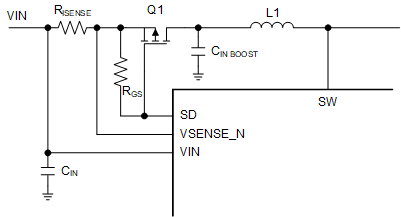
LP8867-Q1 LP8869-Q1 fb-06-PL-FET.gifFigure 14. Power-Line FET Control Schematics

The LP886x-Q1 turns off the power-line FET and prevents the possible boost and LEDs leakage when the device is disabled or in FAULT RECOVERY state.

Power-line FET control is an optional feature. Leave SD pin NC and don't use power-line FET when this feature is not needed.