SLAS701B November 2010 – June 2018 MSP430AFE221 , MSP430AFE222 , MSP430AFE223 , MSP430AFE231 , MSP430AFE232 , MSP430AFE233 , MSP430AFE251 , MSP430AFE252 , MSP430AFE253
PRODUCTION DATA.
- 1Device Overview
- 2Revision History
- 3Device Comparison
- 4Terminal Configuration and Functions
-
5Specifications
- 5.1 Absolute Maximum Ratings
- 5.2 ESD Ratings
- 5.3 Recommended Operating Conditions
- 5.4 Thermal Resistance Characteristics for PW-24 Package
- 5.5 Active Mode Supply Current (Into DVCC and AVCC) Excluding External Current
- 5.6 Typical Characteristics – Active-Mode Supply Current (Into DVCC and AVCC)
- 5.7 Low-Power-Mode Supply Currents (Into VCC) Excluding External Current
- 5.8 Typical Characteristics – LPM4 Current
- 5.9 Schmitt-Trigger Inputs (Ports Px and RST/NMI)
- 5.10 Leakage Current (Ports Px)
- 5.11 Outputs (Ports Px)
- 5.12 Output Frequency (Ports Px)
- 5.13 Typical Characteristics – Outputs
- 5.14 POR, BOR
- 5.15 Typical Characteristics – POR, BOR
- 5.16 Supply Voltage Supervisor (SVS), Supply Voltage Monitor (SVM)
- 5.17 Main DCO Characteristics
- 5.18 DCO Frequency
- 5.19 Calibrated DCO Frequencies – Tolerance
- 5.20 Wake-up Times From Lower-Power Modes (LPM3, LPM4)
- 5.21 Typical Characteristics – DCO Clock Wake-up Time
- 5.22 Internal Very-Low-Power Low-Frequency Oscillator (VLO)
- 5.23 Crystal Oscillator (XT2)
- 5.24 Typical Characteristics – XT2 Oscillator
- 5.25 SD24_A, Power Supply
- 5.26 SD24_A, Input Range
- 5.27 SD24_A, Performance
- 5.28 SD24_A, Temperature Sensor and Built-In VCC Sense
- 5.29 SD24_A, Built-In Voltage Reference
- 5.30 SD24_A, Reference Output Buffer
- 5.31 SD24_A, External Reference Input
- 5.32 USART0
- 5.33 Timer_A3
- 5.34 Flash Memory
- 5.35 RAM
- 5.36 JTAG and Spy-Bi-Wire Interface
- 5.37 JTAG Fuse
-
6Detailed Description
- 6.1 CPU
- 6.2 Instruction Set
- 6.3 Operating Modes
- 6.4 Interrupt Vector Addresses
- 6.5 Special Function Registers
- 6.6 Memory Organization
- 6.7 Flash Memory
- 6.8 Peripherals
- 6.9 Oscillator and System Clock
- 6.10 Brownout, Supply Voltage Supervisor
- 6.11 Digital I/O
- 6.12 Watchdog Timer (WDT+)
- 6.13 Timer_A3
- 6.14 USART0
- 6.15 Hardware Multiplier
- 6.16 SD24_A
- 6.17 Peripheral File Map
- 6.18
I/O Port Schematics
- 6.18.1 Port P1 Pin Schematic: P1.0 Input/Output With Schmitt Trigger
- 6.18.2 Port P1 Pin Schematic: P1.1 and P1.2 Input/Output With Schmitt Trigger
- 6.18.3 Port P1 Pin Schematic: P1.3 Input/Output With Schmitt Trigger
- 6.18.4 Port P1 Pin Schematic: P1.4 Input/Output With Schmitt Trigger
- 6.18.5 Port P1 Pin Schematic: P1.5 to P1.7 Input/Output With Schmitt Trigger
- 6.18.6 Port P2 Pin Schematic: P2.0 Input/Output With Schmitt Trigger
- 6.18.7 Port P2 Pin Schematic: P2.6, Input/Output With Schmitt Trigger
- 6.18.8 Port P2 Pin Schematic: P2.7, Input/Output With Schmitt Trigger
- 6.18.9 JTAG Fuse Check Mode
- 7Device and Documentation Support
- 8Mechanical, Packaging, and Orderable Information
Package Options
Mechanical Data (Package|Pins)
- PW|24
Thermal pad, mechanical data (Package|Pins)
Orderable Information
5.3 Recommended Operating Conditions(1)(2)
| MIN | NOM | MAX | UNIT | ||||
|---|---|---|---|---|---|---|---|
| VCC | Supply voltage | AVCC = DVCC = VCC(1) | During program execution(3) | 1.8 | 3.6 | V | |
| During program or erase of flash memory | 2.2 | 3.6 | |||||
| VSS | Supply voltage | AVSS = DVSS = VSS | 0 | V | |||
| TA | Operating free-air temperature | –40 | 85 | °C | |||
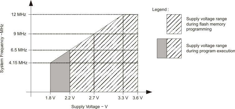
| fSYSTEM | Processor frequency
(maximum MCLK frequency)(1)(2) (see Figure 5-1) |
VCC = 1.8 V, Duty cycle = 50% ±10% | dc | 4.15 | MHz | ||
| VCC = 2.7 V, Duty cycle = 50% ±10% | dc | 9 | |||||
| VCC ≥ 3.3 V, Duty cycle = 50% ±10% | dc | 12 | |||||
(1) The MSP430 CPU is clocked directly with MCLK. Both the high and low phases of MCLK must not exceed the pulse duration of the specified maximum frequency.
(2) Modules might have a different maximum input clock specification. See the specification of the respective module in this data sheet.
(3) The operating voltage range for SD24_A is 2.5 V to 3.6 V

A. Minimum processor frequency is defined by system clock. Flash program or erase operations require a minimum VCC of 2.2 V.
B. If high frequency crystal used is above 12 MHz and selected to source CPU clock then MCLK divider should be programmed appropriately to run CPU below 8 MHz.
Figure 5-1 Operating Area