SLAS396D July 2003 – November 2016 MSP430FE423 , MSP430FE425 , MSP430FE427
PRODUCTION DATA.
- 1Device Overview
- 2Revision History
- 3Device Comparison
- 4Terminal Configuration and Functions
-
5Specifications
- 5.1 Absolute Maximum Ratings
- 5.2 ESD Ratings
- 5.3 Recommended Operating Conditions
- 5.4 Supply Current Into AVCC and DVCC Excluding External Current
- 5.5 Thermal Resistance Characteristics, PM Package (LQFP64)
- 5.6 Schmitt-Trigger Inputs − Ports (P1 and P2), RST/NMI, JTAG (TCK, TMS, TDI/TCLK,TDO/TDI)
- 5.7 Inputs P1.x, P2.x, TAx
- 5.8 Leakage Current − Ports (P1 and P2)
- 5.9 Outputs − Ports (P1 and P2)
- 5.10 Output Frequency
- 5.11 Typical Characteristics - Ports P1 and P2
- 5.12 Wake-up Time From LPM3
- 5.13 RAM
- 5.14 LCD
- 5.15 USART0
- 5.16 POR, BOR
- 5.17 SVS (Supply Voltage Supervisor and Monitor)
- 5.18 DCO
- 5.19 Crystal Oscillator, LFXT1 Oscillator
- 5.20 ESP430CE1, SD16 and ESP430 Power Supply and Operating Conditions
- 5.21 ESP430CE1, SD16 Input Range
- 5.22 ESP430CE1, SD16 Performance
- 5.23 ESP430CE1, SD16 Temperature Sensor
- 5.24 ESP430CE1, SD16 Built-in Voltage Reference
- 5.25 ESP430CE1, SD16 Reference Output Buffer
- 5.26 ESP430CE1, SD16 External Reference Input
- 5.27 ESP430CE1, Active Energy Measurement Test Conditions and Accuracy
- 5.28 ESP430CE1, Active Energy Measurement Test Conditions and Accuracy
- 5.29 ESP430CE1 Typical Characteristics (I1 SD16GAINx = 1)
- 5.30 ESP430CE1 Typical Characteristics (I1 SD16GAINx = 4)
- 5.31 ESP430CE1 Typical Characteristics (I1 SD16GAINx = 8)
- 5.32 ESP430CE1 Typical Characteristics (I1 SD16GAINx = 32)
- 5.33 Flash Memory
- 5.34 JTAG Interface
- 5.35 JTAG Fuse
-
6Detailed Description
- 6.1 CPU
- 6.2 Instruction Set
- 6.3 Operating Modes
- 6.4 Interrupt Vector Addresses
- 6.5 Special Function Registers
- 6.6 Memory Organization
- 6.7 Bootloader (BSL)
- 6.8 Flash Memory
- 6.9 Peripherals
- 6.10
Input/Output Diagrams
- 6.10.1 Port P1 (P1.0 and P1.1) Input/Output With Schmitt Trigger
- 6.10.2 Port P1 (P1.2 to P1.7) Input/Output With Schmitt Trigger
- 6.10.3 Port P2 (P2.0 and P2.1) Input/Output With Schmitt Trigger
- 6.10.4 Port P2 (P2.2 to P2.5) Input/Output With Schmitt Trigger
- 6.10.5 Port P2 (P2.6 and P2.7) Unbonded GPIOs
- 6.10.6 JTAG Pins TMS, TCK, TDI/TCLK, TDO/TDI, Input/Output With Schmitt-Trigger or Output
- 6.10.7 JTAG Fuse Check Mode
- 7Device and Documentation Support
- 8Mechanical, Packaging, and Orderable Information
Package Options
Mechanical Data (Package|Pins)
- PM|64
Thermal pad, mechanical data (Package|Pins)
Orderable Information
1 Device Overview
1.1 Features
- Low Supply Voltage Range: 2.7 V to 3.6 V
- Ultra-Low Power Consumption:
- Active Mode: 400 µA at 1 MHz, 3 V
- Standby Mode: 1.6 µA
- Off Mode (RAM Retention): 0.1 µA
- Five Power-Saving Modes
- Wake up From Standby Mode in Less Than 6 µs
- Frequency-Locked Loop, FLL+
- 16-Bit RISC Architecture, 125-ns Instruction Cycle Time
- Embedded Signal Processing for Single-Phase Energy Metering With Integrated Analog Front End and Temperature Sensor (ESP430CE1)
- 16-Bit Timer_A With Three Capture/Compare Registers
- Integrated LCD Driver for 128 Segments
- Serial Communication Interface (USART), Asynchronous UART or Synchronous SPI Selectable by Software
- Brownout Detector
- Supply Voltage Supervisor and Monitor With Programmable Level Detection
- Serial Onboard Programming, No External Programming Voltage Needed, Programmable Code Protection by Security Fuse
- Bootloader (BSL)
- Family Members Include:
- MSP430FE423
8KB + 256 B of Flash Memory, 256 B of RAM - MSP430FE425
16KB + 256 B of Flash Memory, 512 B of RAM - MSP430FE427
32KB + 256 B of Flash Memory, 1KB of RAM
- MSP430FE423
- Available in 64-Pin Quad Flat Pack (LQFP)
- For Complete Module Descriptions, See the MSP430x4xx Family User's Guide
1.2 Applications
- 2-Wire and 3-Wire Single-Phase Meters
- Tamper-Resistant Meters
1.3 Description
The TI MSP430™ family of ultra-low-power microcontrollers consists of several devices featuring different sets of peripherals targeted for various applications. The architecture, combined with five low-power modes, is optimized to achieve extended battery life in portable measurement applications. The device features a powerful 16-bit RISC CPU, 16-bit registers, and constant generators that contribute to maximum code efficiency. The digitally controlled oscillator (DCO) allows the device to wake up from low-power modes to active mode in less than 6 µs.
The MSP430FE42x series are microcontroller configurations with three independent 16-bit sigma-delta ADCs and an embedded signal processor core used to measure and calculate single-phase energy in both 2-wire and 3-wire configurations. Also included are a built-in 16-bit timer, 128-segment LCD drive capability, and 14 I/O pins.
Typical applications include 2-wire and 3-wire single-phase metering including tamper-resistant meter implementations.
Device Information(1)
| PART NUMBER | PACKAGE | BODY SIZE(2) |
|---|---|---|
| MSP430FE427IPM | LQFP (64) | 10 mm × 10 mm |
| MSP430FE425IPM | LQFP (64) | 10 mm × 10 mm |
| MSP430FE423IPM | LQFP (64) | 10 mm × 10 mm |
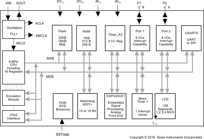
1.4 Functional Block Diagram
Figure 1-1 shows the functional block diagram.
 Figure 1-1 MSP430FE42x Block Diagram