SBOS705D January   2016  – Feburary 2019 MUX36D04 , MUX36S08

PRODUCTION DATA.  

  1. Features
  2. Applications
  3. Description
    1.     Device Images
      1.      Simplified Schematic
      2.      Leakage Current vs Temperature
  4. Revision History
  5. Device Comparison Table
  6. Pin Configuration and Functions
    1.     Pin Functions: MUX36S08
    2.     Pin Functions: MUX36D04
  7. Specifications
    1. 7.1 Absolute Maximum Ratings
    2. 7.2 ESD Ratings
    3. 7.3 Recommended Operating Conditions
    4. 7.4 Thermal Information
    5. 7.5 Electrical Characteristics: Dual Supply
    6. 7.6 Electrical Characteristics: Single Supply
    7. 7.7 Typical Characteristics
  8. Parameter Measurement Information
    1. 8.1  Truth Tables
    2. 8.2  On-Resistance
    3. 8.3  Off-Leakage Current
    4. 8.4  On-Leakage Current
    5. 8.5  Differential On-Leakage Current
    6. 8.6  Transition Time
    7. 8.7  Break-Before-Make Delay
    8. 8.8  Turn-On and Turn-Off Time
    9. 8.9  Charge Injection
    10. 8.10 Off Isolation
    11. 8.11 Channel-to-Channel Crosstalk
    12. 8.12 Bandwidth
    13. 8.13 THD + Noise
  9. Detailed Description
    1. 9.1 Overview
    2. 9.2 Functional Block Diagram
    3. 9.3 Feature Description
      1. 9.3.1 Ultralow Leakage Current
      2. 9.3.2 Ultralow Charge Injection
      3. 9.3.3 Bidirectional Operation
      4. 9.3.4 Rail-to-Rail Operation
    4. 9.4 Device Functional Modes
  10. 10Application and Implementation
    1. 10.1 Application Information
    2. 10.2 Typical Application
      1. 10.2.1 Design Requirements
      2. 10.2.2 Detailed Design Procedure
      3. 10.2.3 Application Curve
  11. 11Power Supply Recommendations
  12. 12Layout
    1. 12.1 Layout Guidelines
    2. 12.2 Layout Example
  13. 13Device and Documentation Support
    1. 13.1 Documentation Support
      1. 13.1.1 Related Documentation
    2. 13.2 Related Links
    3. 13.3 Receiving Notification of Documentation Updates
    4. 13.4 Community Resources
    5. 13.5 Trademarks
    6. 13.6 Electrostatic Discharge Caution
    7. 13.7 Glossary
  14. 14Mechanical, Packaging, and Orderable Information

Package Options

Mechanical Data (Package|Pins)
Thermal pad, mechanical data (Package|Pins)
Orderable Information

Charge Injection

The MUX36xxx have a simple transmission-gate topology. Any mismatch in capacitance between the NMOS and PMOS transistors results in a charge injected into the drain or source during the falling or rising edge of the gate signal. The amount of charge injected into the source or drain of the device is known as charge injection, and is denoted by the symbol QINJ. Figure 33 shows the setup used to measure charge injection.
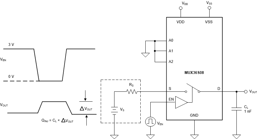
MUX36S08 MUX36D04 Charge_Injection_sbos705.gifFigure 33. Charge-Injection Measurement Setup