SBOS705D January 2016 – Feburary 2019 MUX36D04 , MUX36S08
PRODUCTION DATA.
- 1 Features
- 2 Applications
- 3 Description
- 4 Revision History
- 5 Device Comparison Table
- 6 Pin Configuration and Functions
- 7 Specifications
-
8 Parameter Measurement Information
- 8.1 Truth Tables
- 8.2 On-Resistance
- 8.3 Off-Leakage Current
- 8.4 On-Leakage Current
- 8.5 Differential On-Leakage Current
- 8.6 Transition Time
- 8.7 Break-Before-Make Delay
- 8.8 Turn-On and Turn-Off Time
- 8.9 Charge Injection
- 8.10 Off Isolation
- 8.11 Channel-to-Channel Crosstalk
- 8.12 Bandwidth
- 8.13 THD + Noise
- 9 Detailed Description
- 10Application and Implementation
- 11Power Supply Recommendations
- 12Layout
- 13Device and Documentation Support
- 14Mechanical, Packaging, and Orderable Information
Package Options
Mechanical Data (Package|Pins)
Thermal pad, mechanical data (Package|Pins)
- RUM|16
Orderable Information
11 Power Supply Recommendations
The MUX36xxx operates across a wide supply range of ±5 V to ±18 V (10 V to 36 V in single-supply mode). They also perform well with unsymmetric supplies such as VDD = 12 V and VSS= –5 V. For reliable operation, use a supply decoupling capacitor ranging between 0.1 µF to 10 µF at both the VDD and VSS pins to ground.
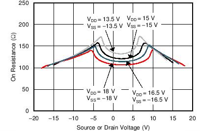
The on-resistance of the MUX36xxx varies with supply voltage, as illustrated in Figure 45
 Figure 45. On-Resistance Variation With Supply and Input Voltage