SBOS705D January 2016 – Feburary 2019 MUX36D04 , MUX36S08
PRODUCTION DATA.
- 1 Features
- 2 Applications
- 3 Description
- 4 Revision History
- 5 Device Comparison Table
- 6 Pin Configuration and Functions
- 7 Specifications
-
8 Parameter Measurement Information
- 8.1 Truth Tables
- 8.2 On-Resistance
- 8.3 Off-Leakage Current
- 8.4 On-Leakage Current
- 8.5 Differential On-Leakage Current
- 8.6 Transition Time
- 8.7 Break-Before-Make Delay
- 8.8 Turn-On and Turn-Off Time
- 8.9 Charge Injection
- 8.10 Off Isolation
- 8.11 Channel-to-Channel Crosstalk
- 8.12 Bandwidth
- 8.13 THD + Noise
- 9 Detailed Description
- 10Application and Implementation
- 11Power Supply Recommendations
- 12Layout
- 13Device and Documentation Support
- 14Mechanical, Packaging, and Orderable Information
Package Options
Mechanical Data (Package|Pins)
Thermal pad, mechanical data (Package|Pins)
- RUM|16
Orderable Information
9.3.2 Ultralow Charge Injection
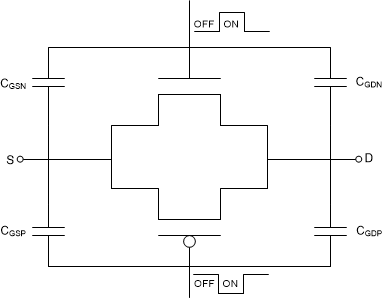
The MUX36xxx have a simple transmission gate topology, as shown in Figure 39. Any mismatch in the stray capacitance associated with the NMOS and PMOS causes an output level change whenever the switch is opened or closed.
 Figure 39. Transmission Gate Topology
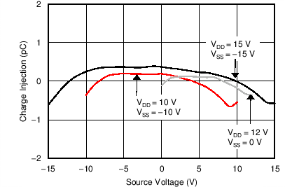
 The MUX36xxx have special charge-injection cancellation circuitry that reduces the source-to-drain charge injection to as low as 0.3 pC at VS = 0 V, and ±0.6 pC in the full signal range, as shown in Figure 40.
 Figure 40. Source-to-Drain Charge Injection vs Source or Drain Voltage
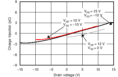
 The drain-to-source charge injection becomes important when the device is used as a demultiplexer (demux), where D becomes the input and Sx becomes the output. Figure 41 shows the drain-to-source charge injection across the full signal range.
 Figure 41. Drain-to-Source Charge Injection vs Source or Drain Voltage