SLASED9C November   2016  – October 2019 MUX36D08 , MUX36S16

PRODUCTION DATA.  

  1. Features
  2. Applications
  3. Description
    1.     Device Images
      1.      Simplified Schematic
      2.      Leakage Current vs Temperature
  4. Revision History
  5. Pin Configuration and Functions
    1.     Pin Functions, MUX36S16
    2.     Pin Functions: MUX36D08
  6. Specifications
    1. 6.1 Absolute Maximum Ratings
    2. 6.2 ESD Ratings
    3. 6.3 Recommended Operating Conditions
    4. 6.4 Thermal Information
    5. 6.5 Electrical Characteristics: Dual Supply
    6. 6.6 Electrical Characteristics: Single Supply
    7. 6.7 Typical Characteristics
  7. Parameter Measurement Information
    1. 7.1 Truth Tables
      1. 7.1.1  On-Resistance
      2. 7.1.2  Off Leakage
      3. 7.1.3  On-Leakage Current
      4. 7.1.4  Differential On-Leakage Current
      5. 7.1.5  Transition Time
      6. 7.1.6  Break-Before-Make Delay
      7. 7.1.7  Turn-On and Turn-Off Time
      8. 7.1.8  Charge Injection
      9. 7.1.9  Off Isolation
      10. 7.1.10 Channel-to-Channel Crosstalk
      11. 7.1.11 Bandwidth
      12. 7.1.12 THD + Noise
  8. Detailed Description
    1. 8.1 Overview
    2. 8.2 Functional Block Diagram
    3. 8.3 Feature Description
      1. 8.3.1 Ultralow Leakage Current
      2. 8.3.2 Ultralow Charge Injection
      3. 8.3.3 Bidirectional Operation
      4. 8.3.4 Rail-to-Rail Operation
    4. 8.4 Device Functional Modes
  9. Application and Implementation
    1. 9.1 Application Information
    2. 9.2 Typical Application
      1. 9.2.1 Design Requirements
      2. 9.2.2 Detailed Design Procedure
      3. 9.2.3 Application Curve
  10. 10Power Supply Recommendations
  11. 11Layout
    1. 11.1 Layout Guidelines
    2. 11.2 Layout Example
  12. 12Device and Documentation Support
    1. 12.1 Documentation Support
      1. 12.1.1 Related Documentation
    2. 12.2 Related Links
    3. 12.3 Receiving Notification of Documentation Updates
    4. 12.4 Community Resources
    5. 12.5 Trademarks
    6. 12.6 Electrostatic Discharge Caution
    7. 12.7 Glossary
  13. 13Mechanical, Packaging, and Orderable Information

Package Options

Mechanical Data (Package|Pins)
Thermal pad, mechanical data (Package|Pins)
Orderable Information

THD + Noise

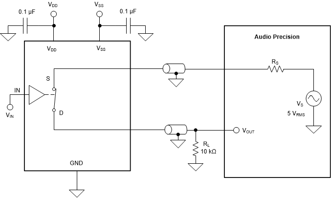
The total harmonic distortion (THD) of a signal is a measurement of the harmonic distortion, and is defined as the ratio of the sum of the powers of all harmonic components to the power of the fundamental frequency at the mux output. The on-resistance of the MUX36xxx varies with the amplitude of the input signal and results in distortion when the drain pin is connected to a low-impedance load. Total harmonic distortion plus noise is denoted as THD+N. Figure 37 shows the setup used to measure THD+N of the MUX36xxx.
MUX36S16 MUX36D08 Audio_Precision.gifFigure 37. THD+N Measurement Setup