SBOS705D January 2016 – Feburary 2019 MUX36D04 , MUX36S08
PRODUCTION DATA.
- 1 Features
- 2 Applications
- 3 Description
- 4 Revision History
- 5 Device Comparison Table
- 6 Pin Configuration and Functions
- 7 Specifications
-
8 Parameter Measurement Information
- 8.1 Truth Tables
- 8.2 On-Resistance
- 8.3 Off-Leakage Current
- 8.4 On-Leakage Current
- 8.5 Differential On-Leakage Current
- 8.6 Transition Time
- 8.7 Break-Before-Make Delay
- 8.8 Turn-On and Turn-Off Time
- 8.9 Charge Injection
- 8.10 Off Isolation
- 8.11 Channel-to-Channel Crosstalk
- 8.12 Bandwidth
- 8.13 THD + Noise
- 9 Detailed Description
- 10Application and Implementation
- 11Power Supply Recommendations
- 12Layout
- 13Device and Documentation Support
- 14Mechanical, Packaging, and Orderable Information
Package Options
Mechanical Data (Package|Pins)
Thermal pad, mechanical data (Package|Pins)
- RUM|16
Orderable Information
8.8 Turn-On and Turn-Off Time
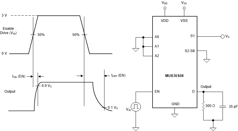
Turn-on time is defined as the time taken by the output of the MUX36xxx to rise to a 90% final value after the enable signal has risen to a 50% final value. Figure 32 shows the setup used to measure turn-on time. Turn-on time is denoted by the symbol tON.
Turn off time is defined as the time taken by the output of the MUX36xxx to fall to a 10% initial value after the enable signal has fallen to a 50% initial value. Figure 32 shows the setup used to measure turn-off time. Turn-off time is denoted by the symbol tOFF.
 Figure 32. Turn-On and Turn-Off Time Measurement Setup