SLOS075J November 1979 – January 2015 NE5532 , NE5532A , SA5532 , SA5532A
PRODUCTION DATA.
- 1 Features
- 2 Applications
- 3 Description
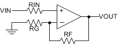
- 4 Simplified Schematic
- 5 Revision History
- 6 Pin Configuration and Functions
- 7 Specifications
- 8 Detailed Description
- 9 Application and Implementation
- 10Power Supply Recommendations
- 11Layout
- 12Device and Documentation Support
- 13Mechanical, Packaging, and Orderable Information
Package Options
Mechanical Data (Package|Pins)
Thermal pad, mechanical data (Package|Pins)
Orderable Information
1 Features
2 Applications
- AV Receivers
- Embedded PCs
- Netbooks
- Video Broadcasting and Infrastructure: Scalable Platforms
- DVD Recorders and Players
- Multichannel Video Transcoders
- Pro Audio Mixers
3 Description
The NE5532, NE5532A, SA5532, and SA5532A devices are high-performance operational amplifiers combining excellent DC and AC characteristics. They feature very low noise, high output-drive capability, high unity-gain and maximum-output-swing bandwidths, low distortion, high slew rate, input-protection diodes, and output short-circuit protection. These operational amplifiers are compensated internally for unity-gain operation. These devices have specified maximum limits for equivalent input noise voltage.
Device Information(1)
| PART NUMBER | PACKAGE (PIN) | BODY SIZE (NOM) |
|---|---|---|
| NE5532x, SA5532x | SOIC (8) | 4.90 mm × 3.91 mm |
| NE5532x, SA5532x | PDIP (8) | 9.81 mm × 6.35 mm |
| NE5532x | SO (8) | 6.20 mm × 5.30 mm |
- For all available packages, see the orderable addendum at the end of the data sheet.
4 Simplified Schematic