SLLSEK1B July   2014  – March 2018 ONET2804T

PRODUCTION DATA.  

  1. Features
  2. Applications
  3. Description
    1.     Device Images
      1.      Simplified Schematic
      2.      Eye Diagram
  4. Revision History
  5. Pin Configuration and Functions
    1.     Bond Pad Functions
  6. Specifications
    1. 6.1 Absolute Maximum Ratings
    2. 6.2 ESD Ratings
    3. 6.3 Recommended Operating Conditions
    4. 6.4 DC Electrical Characteristics
    5. 6.5 AC Electrical Characteristics
    6. 6.6 Typical Characteristics
  7. Detailed Description
    1. 7.1 Overview
    2. 7.2 Functional Block Diagram
    3. 7.3 Feature Description
      1. 7.3.1 Signal Path
      2. 7.3.2 Gain Adjustment
      3. 7.3.3 Amplitude Adjustment
      4. 7.3.4 Rate Select
      5. 7.3.5 Threshold Adjustment
      6. 7.3.6 Filter Circuitry
      7. 7.3.7 AGC and RSSI
    4. 7.4 Device Functional Modes
      1. 7.4.1 Pad Control
      2. 7.4.2 2-Wire Interface Control
      3. 7.4.3 2-Wire Interface and Control Logic
      4. 7.4.4 Bus Idle
      5. 7.4.5 Start Data Transfer
      6. 7.4.6 Stop Data Transfer
      7. 7.4.7 Data Transfer
      8. 7.4.8 Acknowledge
    5. 7.5 Register Maps
      1. 7.5.1  Register 0 (0x00) – Control Settings (offset = 0h) [reset = 0h]
        1. Table 2. Register 0 (0x00) – Control Settings Field Descriptions
      2. 7.5.2  Register 1 (0x01) – Amplitude and Rate for Channel 1 (offset = 1h) [reset = 0h]
        1. Table 3. Register 1 (0x01) – Amplitude and Rate for Channel 1 Field Descriptions
      3. 7.5.3  Register 2 (0x02) Mapping – Threshold and Gain for Channel 1 (offset = 2h) [reset = 0h]
        1. Table 4. Register 2 (0x02) – Threshold and Gain for Channel 1
      4. 7.5.4  Register 3 (0x03) – Reserved
        1. Table 5. Register 3 (0x03) – Reserved Field Descriptions
      5. 7.5.5  Register 4 (0x04) – Reserved
        1. Table 6. Register 4 (0x04) – Reserved Field Descriptions
      6. 7.5.6  Register 5 (0x05) – Reserved
        1. Table 7. Register 5 (0x05) – Reserved Field Descriptions
      7. 7.5.7  Register 6 (0x06) – Reserved
        1. Table 8. Register 6 (0x06) – Reserved Field Descriptions
      8. 7.5.8  Register 7 (0x07) – Amplitude and Rate for Channel 2 (offset = 7h) [reset = 0h]
        1. Table 9. Register 7 (0x07) – Amplitude and Rate for Channel 2 Field Descriptions
      9. 7.5.9  Register 8 (0x08) Mapping – Threshold and Gain for Channel 1 (offset = 8h) [reset = 0h]
        1. Table 10. Register 8 (0x08) – Threshold and Gain for Channel 2
      10. 7.5.10 Register 9 (0x09) – Reserved
        1. Table 11. Register 9 (0x09) – Reserved Field Descriptions
      11. 7.5.11 Register 10 (0x0A) – Reserved
        1. Table 12. Register 10 (0x0A) – Reserved Field Descriptions
      12. 7.5.12 Register 11 (0x0B) – Reserved
        1. Table 13. Register 11 (0x0B) – Reserved Field Descriptions
      13. 7.5.13 Register 12 (0x0C) – Reserved
        1. Table 14. Register 12 (0x0C) – Reserved Field Descriptions
      14. 7.5.14 Register 13 (0x0D) – Amplitude and Rate for Channel 3 (offset = Dh) [reset = 0h]
        1. Table 15. Register 13 (0x0D) – Amplitude and Rate for Channel 3 Field Descriptions
      15. 7.5.15 Register 14 (0x0E) Mapping – Threshold and Gain for Channel 3 (offset = Eh) [reset = 0h]
        1. Table 16. Register 14 (0x0E) – Threshold and Gain for Channel 3
      16. 7.5.16 Register 15 (0x0F) – Reserved
        1. Table 17. Register 15 (0x0F) – Reserved Field Descriptions
      17. 7.5.17 Register 16 (0x10) – Reserved
        1. Table 18. Register 16 (0x10) – Reserved Field Descriptions
      18. 7.5.18 Register 17 (0x11) – Reserved
        1. Table 19. Register 17 (0x11) – Reserved Field Descriptions
      19. 7.5.19 Register 18 (0x12) – Reserved
        1. Table 20. Register 18 (0x12) – Reserved Field Descriptions
      20. 7.5.20 Register 19 (0x13) – Amplitude and Rate for Channel 4 (offset = 13h ) [reset = 0h]
        1. Table 21. Register 19 (0x13) – Amplitude and Rate for Channel 4 Field Descriptions
      21. 7.5.21 Register 20 (0x14) Mapping – Threshold and Gain for Channel 4 (offset =14h) [reset = 0h]
        1. Table 22. Register 20 (0x14) – Threshold and Gain for Channel 4
      22. 7.5.22 Register 21 (0x15) – Reserved
        1. Table 23. Register 21 (0x15) – Reserved Field Descriptions
      23. 7.5.23 Register 22 (0x10) – Reserved
        1. Table 24. Register 21 (0x10) – Reserved Field Descriptions
      24. 7.5.24 Register 23 (0x17) – Reserved
        1. Table 25. Register 23 (0x17) – Reserved Field Descriptions
      25. 7.5.25 Register 24 (0x18) – Reserved
        1. Table 26. Register 24 (0x18) – Reserved Field Descriptions
      26. 7.5.26 Register 25 (0x19) – Reserved
        1. Table 27. Register 25 (0x19) – Reserved Field Descriptions
  8. Application and Implementation
    1. 8.1 Application Information
    2. 8.2 Typical Applications
      1. 8.2.1 Typical Application, Pad Control
        1. 8.2.1.1 Design Requirements
        2. 8.2.1.2 Detailed Design Procedure
        3. 8.2.1.3 Application Curves
      2. 8.2.2 Typical Application, 2-Wire Control
        1. 8.2.2.1 Design Requirements
        2. 8.2.2.2 Detailed Design Procedure
        3. 8.2.2.3 Application Curves
  9. Power Supply Recommendations
  10. 10Layout
    1. 10.1 Layout Guidelines
    2. 10.2 Layout Example
  11. 11Device and Documentation Support
    1. 11.1 Receiving Notification of Documentation Updates
    2. 11.2 Community Resources
    3. 11.3 Trademarks
    4. 11.4 Electrostatic Discharge Caution
    5. 11.5 Glossary
  12. 12Mechanical, Packaging, and Orderable Information

Package Options

Mechanical Data (Package|Pins)
  • Y|0
Thermal pad, mechanical data (Package|Pins)
Orderable Information

Pin Configuration and Functions

Bond Pad Assignment of ONET2804T
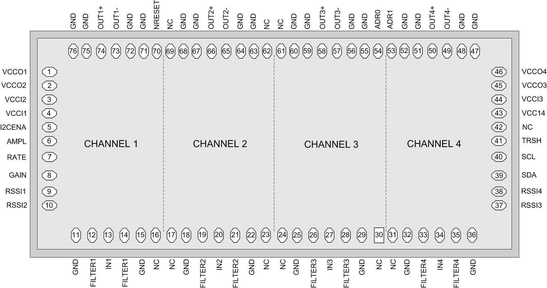
ONET2804T Padout_SLLSEK1.gif

Bond Pad Functions

PAD SYMBOL TYPE DESCRIPTION
6 AMPL Digital input 3-state input for amplitude control of all 4 channels.
VCC: 500 mVpp differential output swing
Open: 300 mVpp differential output swing (default)
GND: 250 mVpp differential output swing.
53 ADR1 Digital input 2-wire interface address programming pin. Leave this pad open for a default address of 0001100. Grounding this pad changes the 2nd address bit to a 1 (0001110).
54 ADR0 Digital input 2-wire interface address programming pin. Leave this pad open for a default address of 0001100. Grounding this pad changes the 1st address bit to a 1 (0001101).
12, 14, 19, 21, 26, 28, 33, 35 FILTERx Analog output Bias voltage for photodiode cathode. These pads are biased to VCC - 100 mV.
8 GAIN Digital input 3-state input for gain control of all 4 channels.
VCC: Minimum transimpedance
Open: Default transimpedance
GND: Medium transimpedance
11, 15, 18, 22, 25, 29, 32, 36, 47, 48, 51, 52, 55, 56, 59, 60, 63, 64, 67, 68, 71, 72, 75, 76 GND Supply Circuit ground. All GND pads are connected on die. Bonding all pads is recommended, except for 11, 15, 18, 22, 25,29,32, and 36.
5 I2CENA Digital input 2-wire control option. Leave the pad unconnected for pad control of the IC. Two-wire control can be enabled by applying a high signal to the pad.
13, 20, 27, 34 INx Analog input Data input to TIAx (connect to photodiode anode).
16, 17, 23, 24, 30, 31, 42, 61, 62, 69 NC No Connect Do not connect
70 NRESET Digital input Used to reset the 2-wire state machine and registers. Leave open for normal operation and set low to reset the 2-wire interface.
49, 57, 65, 73 OUTx– Analog output Inverted CML data output for channel x. On-chip 50 Ω back-terminated to VCC.
50, 58, 66, 74 OUTx+ Analog output Non-inverted CML data output for channel x. On-chip 50 Ω back-terminated to VCC.
7 RATE Digital input 3-state input for bandwidth control of all 4 channels.
VCC: Increase the bandwidth
Open: 21 GHz bandwidth (default)
GND: reduce the bandwidth
9, 10, 37, 38 RSSIx Analog output Indicates the strength of the received signal (RSSI) for channel x if the photo diode is biased from FILTERx. The analog output current is proportional to the input data amplitude. Connect to an external resistor to ground (GND). For proper operation, ensure that the voltage at the RSSI pad does not exceed VCC - 0.65 V. If the RSSI feature is not used these pads should be left open.
40 SCL Digital input 2-wire interface serial clock input. Includes a 10 kΩ pull-up resistor to VCC.
39 SDA Digital –in/out 2-wire interface serial data input. Includes a 10 kΩ pull-up resistor to VCC.
41 TRSH Digital input 3-state input for threshold control.
VCC: Crossing point shifted down
Open: No threshold adjustment (default)
GND: Crossing point shifted up
1, 2, 45, 46 VCCOx Supply 2.97 V – 3.47 V supply voltage for AGCx and CMLx amplifiers.
3, 4, 43, 44 VCCIx Supply 2.97 V – 3.47 V supply voltage for input TIAx stage.