SBAS796 July 2017 ONET2804TLP
PRODUCTION DATA.
- 1 Features
- 2 Applications
- 3 Description
- 4 Revision History
- 5 Pin Configuration and Functions
- 6 Specifications
-
7 Detailed Description
- 7.1 Overview
- 7.2 Functional Block Diagram
- 7.3 Feature Description
- 7.4 Device Functional Modes
- 7.5 Programming
- 7.6
Register Maps
- 7.6.1 Register Descriptions
- 7.6.2 Register 0: Control Settings (address = 00h) [reset = 0h]
- 7.6.3 Register 1: Amplitude and Rate for Channel 1 (address = 01h) [reset = 0h]
- 7.6.4 Register 2: Threshold and Gain for Channel 1 (address = 02h) [reset = 0h]
- 7.6.5 Register 7: Amplitude and Rate for Channel 2 (address = 07h) [reset = 0h]
- 7.6.6 Register 8: Threshold and Gain for Channel 1 (address = 08h) [reset = 0h]
- 7.6.7 Register 13: Amplitude and Rate for Channel 3 (address = 0Dh) [reset = 0h]
- 7.6.8 Register 14: Threshold and Gain for Channel 3 (address = 0Eh) [reset = 0h]
- 7.6.9 Register 19: Amplitude and Rate for Channel 4 (address = 13h) [reset = 0h]
- 7.6.10 Register 20: Threshold and Gain for Channel 4 (address = 14h) [reset = 0h]
- 8 Application and Implementation
- 9 Power Supply Recommendations
- 10Layout
- 11Device and Documentation Support
- 12Mechanical, Packaging, and Orderable Information
Package Options
Mechanical Data (Package|Pins)
- Y|0
Thermal pad, mechanical data (Package|Pins)
Orderable Information
1 Features
- 4-Channel Multi-Rate Operation: Up to 28 Gbps
- Dissipation at a 3-V Supply: 90 mW per Channel
- Differential Transimpedance: 7.5 kΩ
- Bandwidth: 17.5 GHz
- Input-Referred Noise: 2 μArms
- Input Overload Current: 3.2 mAPP
- Programmable Output Voltage
- Adjustable Gain and Bandwidth
- Received Signal Strength Indicator (RSSI) for Each Channel
- Isolation Between Channels (Die Only): 40 dB
- Single Supply: 2.8 V to 3.3 V
- Pad Control or 2-Wire Control
- On-Chip Filter Capacitors
- –40°C to +100°C Operation
- Die Size: 3250 μm × 1450 μm, 750-μm Channel Pitch
2 Applications
- 100 Gigabit Ethernet Optical Receivers
- ITU OTL4.4
- CFP2, CFP4, and QSFP28 Modules with Internal Retiming
3 Description
The ONET2804TLP device is a high-gain, limiting transimpedance amplifier (TIA) for parallel optical interconnects with data rates up to 28 Gbps. The device is used in conjunction with a 750-μm pitch photodiode array to convert an optical signal into a differential output voltage. An internal circuit provides the photodiode reverse bias voltage and senses the average photocurrent supplied to each photodiode.
The device can be used with pin control or a two-wire serial interface to allow control of the output amplitude, gain, bandwidth, and input threshold.
The ONET2804TLP provides 17.5-GHz bandwidth, a gain of 7.5 kΩ, an input-referred noise of 2 µArms, and a received signal strength indicator (RSSI) for each channel. 40-dB isolation between channels results in low crosstalk penalty in the receiver.
The device requires a single 2.8-V to 3.3-V supply and typically dissipates 90 mW per channel with a differential output amplitude of 300 mVPP. The device is characterized for operation from –40°C to +100°C and is available in die form with a 750-μm channel pitch.
Device Information(1)
| PART NUMBER | PACKAGE | BODY SIZE (NOM) |
|---|---|---|
| ONET2804TLP | Base Die in Waffle Pack | 3250 µm × 1450 µm |
- For all available packages, see the orderable addendum at the end of the datasheet.
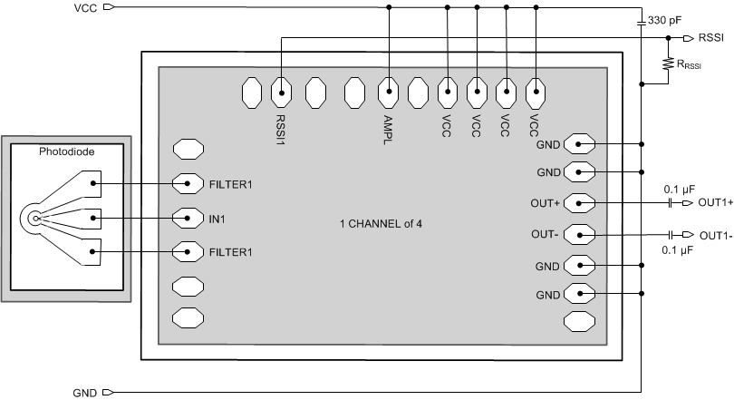
Simplified Schematic

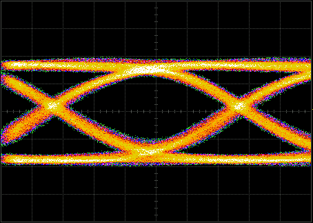
Eye Diagram
