SBOS789C August   2017  – February 2020 OPA2810

PRODUCTION DATA.  

  1. Features
  2. Applications
  3. Description
    1.     Device Images
      1.      Multichannel Sensor Interface
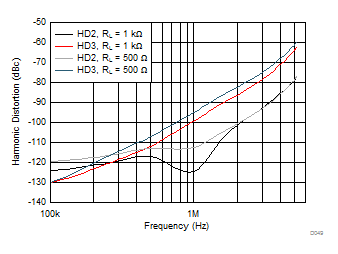
      2.      Harmonic Distortion vs Frequency
  4. Revision History
  5. Device Comparison Table
  6. Pin Configuration and Functions
    1.     Pin Functions
  7. Specifications
    1. 7.1  Absolute Maximum Ratings
    2. 7.2  ESD Ratings
    3. 7.3  Recommended Operating Conditions
    4. 7.4  Thermal Information
    5. 7.5  Electrical Characteristics: 10 V
    6. 7.6  Electrical Characteristics: 24 V
    7. 7.7  Electrical Characteristics: 5 V
    8. 7.8  Typical Characteristics: VS = 10 V
    9. 7.9  Typical Characteristics: VS = 24 V
    10. 7.10 Typical Characteristics: VS = 5 V
    11. 7.11 Typical Characteristics: ±2.375 V to ±12 V Split Supply
  8. Detailed Description
    1. 8.1 Overview
    2. 8.2 Functional Block Diagram
    3. 8.3 Feature Description
      1. 8.3.1 OPA2810 Architecture
      2. 8.3.2 ESD Protection
    4. 8.4 Device Functional Modes
      1. 8.4.1 Split-Supply Operation (±2.375 V to ±13.5 V)
      2. 8.4.2 Single-Supply Operation (4.75 V to 27 V)
  9. Application and Implementation
    1. 9.1 Application Information
      1. 9.1.1 Selection of Feedback Resistors
      2. 9.1.2 Noise Analysis and the Effect of Resistor Elements on Total Noise
    2. 9.2 Typical Applications
      1. 9.2.1 Transimpedance Amplifier
        1. 9.2.1.1 Design Requirements
        2. 9.2.1.2 Detailed Design Procedure
      2. 9.2.2 Multichannel Sensor Interface
  10. 10Power Supply Recommendations
  11. 11Layout
    1. 11.1 Layout Guidelines
      1. 11.1.1 Thermal Considerations
    2. 11.2 Layout Example
  12. 12Device and Documentation Support
    1. 12.1 Documentation Support
      1. 12.1.1 Related Documentation
    2. 12.2 Receiving Notification of Documentation Updates
    3. 12.3 Community Resources
    4. 12.4 Trademarks
    5. 12.5 Electrostatic Discharge Caution
    6. 12.6 Glossary
  13. 13Mechanical, Packaging, and Orderable Information

Package Options

Mechanical Data (Package|Pins)
Thermal pad, mechanical data (Package|Pins)
Orderable Information

Typical Characteristics: VS = 10 V

at VS+ = 5 V, VS– = –5 V, RL = 1 kΩ, input and output are biased to midsupply, and TA ≈ 25°C. For AC specifications, VO = 2 VPP, G = 2 V/V, RF = 1 kΩ, and CL = 4.7 pF (unless otherwise noted)
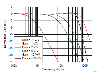
OPA2810 D041_SBOS789_SSBW_Vs_Gain_10V.gif
See Figure 64 and Figure 65, VO = 20 mVPP
Figure 1. Small-Signal Frequency Response vs Gain
OPA2810 D043_SBOS789_SSBW_Vs_Rload_gain2_10V.gif
See Figure 64, VO = 20 mVPP, Gain = 2 V/V
Figure 3. Small-Signal Frequency Response vs Output Load
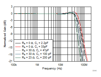
OPA2810 D045_SBOS789_SSBW_Vs_Cload_gain2_10V.gif
See Figure 64and Figure 62, VO = 20 mVPP, Gain = 2 V/V
Figure 5. Small-Signal Frequency Response vs CL
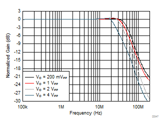
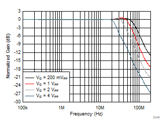
OPA2810 D047_SBOS789_LSBW_Vs_Vout_gain2_10V.gif
See Figure 64, Gain = 2 V/V
Figure 7. Large-Signal Frequency Response vs Output Voltage
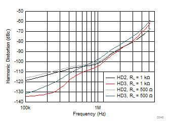
OPA2810 D048_SBOS789_HD_Vs_Freq_RL_gain2_10V.gif
See Figure 64, Gain = 2 V/V
Figure 9. Harmonic Distortion vs Frequency
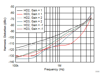
OPA2810 D050_SBOS789_HD_Vs_Freq_Gain_10V.gif
See Figure 64 and Figure 65, RF = 0 Ω for Gain = 1 V/V
Figure 11. Harmonic Distortion vs Gain
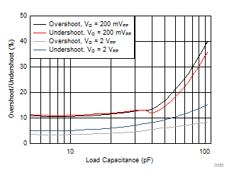
OPA2810 D053_SBOS789_OvershootUndershoot_Vs_Cout_10V.gif
See Figure 64, Gain = 1 V/V, RF = 0 Ω
Figure 13. Overshoot and Undershoot vs CL
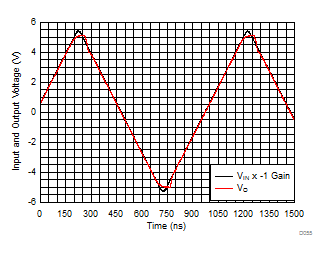
OPA2810 D055_SBOS789_Output_Overdrive_5V.gif
See Figure 65, Gain = -1 V/V
Figure 15. Output Overdrive Recovery
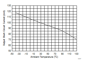
OPA2810 D057_SBOS789_SCCurrent_vs_temp_10V.gif
Output saturated and then short-circuited, Io measured after
TDelay = 5 msec
Figure 17. Output Short-Circuit Current vs Ambient Temperature
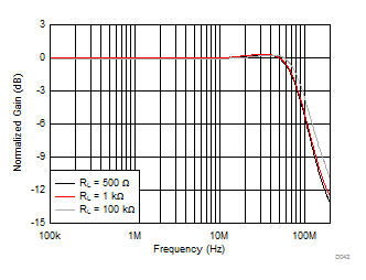
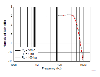
OPA2810 D042_SBOS789_SSBW_Vs_Rload_gain1_10V.gif
See Figure 64, VO = 20 mVPP, Gain = 1 V/V, RF = 0 Ω
Figure 2. Small-Signal Frequency Response vs Output Load
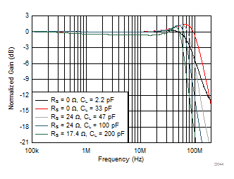
OPA2810 D044_SBOS789_SSBW_Vs_Cload_gain1_10V.gif
See Figure 64 and Figure 62,
VO = 20 mVPP, Gain = 1 V/V, RF = 0 Ω
Figure 4. Small-Signal Frequency Response vs CL
OPA2810 D046_SBOS789_LSBW_Vs_Vout_gain1_10V.gif
See Figure 64, Gain = 1 V/V, RF = 0 Ω
Figure 6. Large-Signal Frequency Response vs Output Voltage
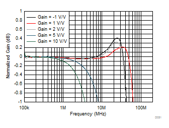
OPA2810 D051_SBOS789_RespFlat_Vs_Gain_10V.gif
See Figure 64 and Figure 65, VO = 20 mVPP
Figure 8. Small-Signal Response Flatness vs Gain
OPA2810 D049_SBOS789_HD_Vs_Freq_RL_gain-1_10V.gif
See Figure 65, Gain = –1 V/V
Figure 10. Harmonic Distortion vs Frequency
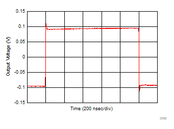
OPA2810 D052_SBOS789_Small_Signal_Transient_200mVpp_10V.gif
See Figure 64, Gain = 1 V/V, RF = 0 Ω
Figure 12. Small-Signal Transient Response
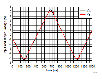
OPA2810 D054_SBOS789_Input_Overdrive_10V.gif
See Figure 64, Gain = 1 V/V, RF = 0 Ω
Figure 14. Input Overdrive Recovery
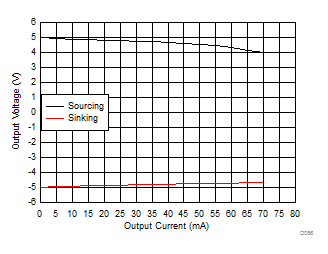
OPA2810 D056_SBOS789_Claw_10V.gif
Figure 16. Output Voltage vs Load Current
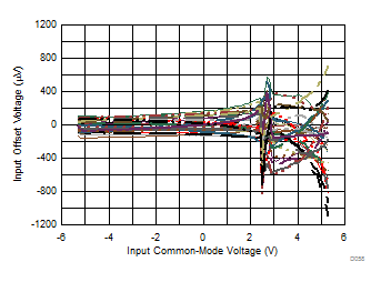
OPA2810 D058_SBOS789_Vos_vs_Vcm.gif
Measured for 34 units
Figure 18. Input Offset Voltage vs Input Common-Mode Voltage