SBOS973A June   2019  – September 2019 OPA2834

PRODUCTION DATA.  

  1. Features
  2. Applications
  3. Description
    1.     Device Images
      1.      1-kHz FFT Plot (VOUT = 1 VRMS, RL = 100 kΩ, G = 1)
      2.      Low-Side, Current-Shunt Monitoring
  4. Revision History
  5. Device Comparison Table
  6. Pin Configuration and Functions
    1.     Pin Functions
  7. Specifications
    1. 7.1 Absolute Maximum Ratings
    2. 7.2 ESD Ratings
    3. 7.3 Recommended Operating Conditions
    4. 7.4 Thermal Information
    5. 7.5 Electrical Characteristics: 3V to 5V
    6. 7.6 Typical Characteristics: Vs = 5 V
    7. 7.7 Typical Characteristics: VS = 3.0 V
    8. 7.8 Typical Characteristics: ±2.5-V to ±1.5-V Split Supply
  8. Detailed Description
    1. 8.1 Overview
    2. 8.2 Functional Block Diagrams
    3. 8.3 Feature Description
      1. 8.3.1 Input Common-Mode Voltage Range
      2. 8.3.2 Output Voltage Range
      3. 8.3.3 Low-Power Applications and the Effects of Resistor Values on Bandwidth
      4. 8.3.4 Driving Capacitive Loads
    4. 8.4 Device Functional Modes
      1. 8.4.1 Split-Supply Operation (±1.35 V to ±2.7 V)
      2. 8.4.2 Single-Supply Operation (2.7 V to 5.4 V)
  9. Application and Implementation
    1. 9.1 Application Information
      1. 9.1.1 Noninverting Amplifier
      2. 9.1.2 Inverting Amplifier
    2. 9.2 Typical Applications
      1. 9.2.1 Low-Side Current Sensing
        1. 9.2.1.1 Design Requirements
        2. 9.2.1.2 Detailed Design Procedure
      2. 9.2.2 Field Transmitter Sensor Interface
      3. 9.2.3 Ultrasonic Flow Meters
      4. 9.2.4 Microphone Pre-Amplifier
  10. 10Power Supply Recommendations
  11. 11Layout
    1. 11.1 Layout Guidelines
    2. 11.2 Layout Examples
  12. 12Device and Documentation Support
    1. 12.1 Documentation Support
      1. 12.1.1 Related Documentation
    2. 12.2 Receiving Notification of Documentation Updates
    3. 12.3 Community Resources
    4. 12.4 Trademarks
    5. 12.5 Electrostatic Discharge Caution
    6. 12.6 Glossary
  13. 13Mechanical, Packaging, and Orderable Information

Package Options

Mechanical Data (Package|Pins)
Thermal pad, mechanical data (Package|Pins)
Orderable Information

Typical Characteristics: Vs = 5 V

VS+ = 5 V, VS– = 0 V, RF = 0 Ω, RL = 5 kΩ, CL = 4 pF, input and output referenced to mid-supply, and TA ≈ 25°C (unless otherwise noted)
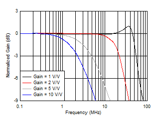
OPA2834 D101_NonInv_5V_SSBW.gif
VO = 20 mVPP
Figure 1. Noninverting Small-Signal Frequency Response
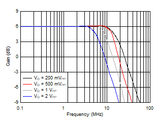
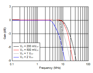
OPA2834 D103_NonInv_5V_LSBW.gif
Gain = 2 V/V
Figure 3. Noninverting Large-Signal Frequency Response
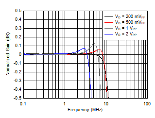
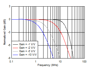
OPA2834 D206_new_5V_noninverting_flatnesslsbw.gif
Gain = 2 V/V
Figure 5. Noninverting Large-Signal Response Flatness
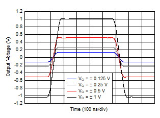
OPA2834 D303_noninverting_Stepresponse_5V.gif
Gain = 2 V/V
Figure 7. Noninverting Step Response
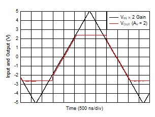
OPA2834 D305_5V_overdrive_noninverting.gif
Gain = 2 V/V
Figure 9. Noninverting Overdrive Recovery
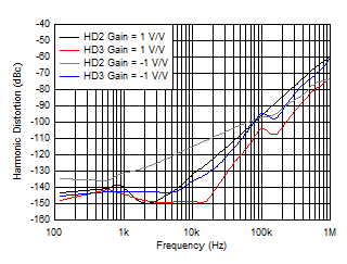
OPA2834 D110_5V_HD_vs_frequency.gif
VO = 2 VPP
Figure 11. Harmonic Distortion vs Frequency
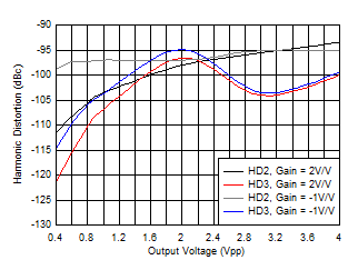
OPA2834 D111_5V_HD_vs_Vout.gif
f = 100 kHz
Figure 13. Harmonic Distortion vs Output Voltage
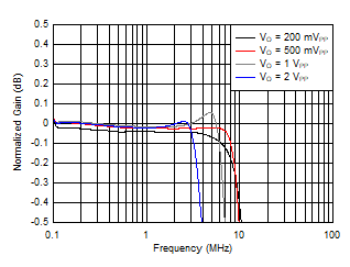
OPA2834 D102_Inv_5V_SSBW.gif
VO = 20 mVPP
Figure 2. Inverting Small-Signal Frequency Response
OPA2834 D104_Inv_5V_LSBW.gif
Gain = –1 V/V
Figure 4. Inverting Large-Signal Frequency Response
OPA2834 D205_NEW_5V_inverting_flatnesslsbw.gif
Gain = –1 V/V
Figure 6. Inverting Large-Signal Response Flatness
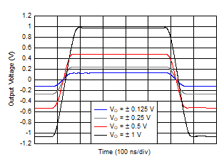
OPA2834 D304_inverting_Stepresponse_5V.gif
Gain = –1 V/V
Figure 8. Inverting Step Response
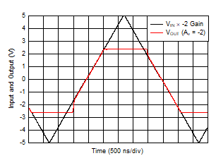
OPA2834 D306_Inv_5V_Overdrive.gif
Gain = –2 V/V
Figure 10. Inverting Overdrive Recovery
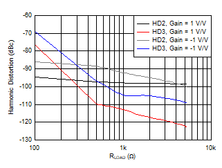
OPA2834 D307_5V_HD_vs_Rload.gif
VO = 2 VPP, f = 100 kHz
Figure 12. Harmonic Distortion vs RLOAD
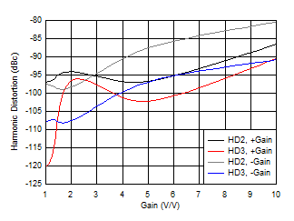
OPA2834 D201_New_5V_HD_vs_Gain.gif
VO = 2 VPP, f = 100 kHz
Figure 14. Harmonic Distortion vs Gain Magnitude