SBOS058A December 1997 – October 2015 OPA134 , OPA2134 , OPA4134
PRODUCTION DATA.
- 1 Features
- 2 Applications
- 3 Description
- 4 Revision History
- 5 Pin Configuration and Functions
- 6 Specifications
- 7 Detailed Description
- 8 Application and Implementation
- 9 Power Supply Recommendations
- 10Layout
- 11Device and Documentation Support
- 12Mechanical, Packaging, and Orderable Information
Package Options
Mechanical Data (Package|Pins)
- D|14
Thermal pad, mechanical data (Package|Pins)
- D|14
Orderable Information
8 Application and Implementation
NOTE
Information in the following applications sections is not part of the TI component specification, and TI does not warrant its accuracy or completeness. TI’s customers are responsible for determining suitability of components for their purposes. Customers should validate and test their design implementation to confirm system functionality.
8.1 Application Information
The OPA134 series operational amplifiers are unity-gain stable, and suitable for a wide range of audio and general-purpose applications. All circuitry is independent in the dual version, assuring normal behavior when one amplifier in a package is overdriven or short-circuited. Power supply pins should be bypassed with 10-nF ceramic capacitors or larger to minimize power supply noise.
8.1.1 Operating Voltage
The OPA134 series of operational amplifiers operate with power supplies from ±2.5 V to ±18 V with excellent performance. Although specifications are production tested with ±15-V supplies, most behavior remains unchanged throughout the full operating voltage range. Parameters which vary significantly with operating voltage are shown in Typical Characteristics.
8.1.2 Offset Voltage Trim
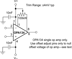
Offset voltage of OPA134 series amplifiers is laser-trimmed, and usually requires no user adjustment. The OPA134 (single operational amplifier version) provides offset trim connections on pins 1 and 8, identical to 5534 amplifiers. Offset voltage can be adjusted by connecting a potentiometer as shown in Figure 29. This adjustment should be used only to null the offset of the operational amplifier, not to adjust system offset or offset produced by the signal source. Nulling offset could change the offset voltage drift behavior of the operational amplifier. While it is not possible to predict the exact change in drift, the effect is usually small.
 Figure 29. OPA134 Offset Voltage Trim Circuit
8.2 Typical Application
The OPAx134 family offers outstanding dc precision and AC performance. These devices operate up to 36-V supply rails and offer ultralow distortion and noise, as well as 8-MHz bandwidth and high capacitive load drive. These features make the OPAx134 a robust, high-performance operational amplifier for high-voltage professional audio applications.
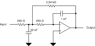
 Figure 30. OPA134 2nd Order 30-kHz, Low Pass Filter Schematic
8.2.1 Design Requirements
- Gain = 5 V/V (inverting)
- Low pass cutoff frequency = 30 kHz
- –40 db/dec filter response
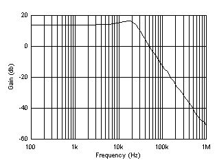
- Maintain less than 3-dB gain peaking in the gain versus frequency response
8.2.2 Detailed Design Procedure
The infinite-gain multiple-feedback circuit for a low-pass network function is shown in Figure 30. The voltage transfer function is:

This circuit produces a signal inversion. For this circuit the gain at DC and the low pass cutoff frequency are calculated using Equation 3.

Software tools are readily available to simplify filter design. WEBENCH® Filter Designer is a simple, powerful, and easy-to-use active filter design program. The WEBENCH Filter Designer lets you create optimized filter designs using a selection of TI operational amplifiers and passive components from TI's vendor partners.
Available as a web based tool from the WEBENCH® Design Center, WEBENCH® Filter Designer allows you to design, optimize, and simulate complete multistage active filter solutions within minutes.
8.2.3 Application Curve
 Figure 31. OPA134 2nd Order 30-kHz, Low Pass Filter Response