SBOS809A November 2016 – June 2017 OPA2172-Q1 , OPA4172-Q1
PRODUCTION DATA.
- 1 Features
- 2 Applications
- 3 Description
- 4 Revision History
- 5 Device Comparison Table
- 6 Pin Configuration and Functions
- 7 Specifications
- 8 Detailed Description
- 9 Applications and Implementation
- 10Power Supply Recommendations
- 11Layout
- 12Device and Documentation Support
- 13Mechanical, Packaging, and Orderable Information
Package Options
Mechanical Data (Package|Pins)
- PW|14
Thermal pad, mechanical data (Package|Pins)
- PW|14
Orderable Information
1 Features
- Qualified for Automotive Applications
- AEC-Q100 Qualified With the Following Results:
- Device Temperature Grade 1:
–40°C to +125°C
Ambient Operating Temperature Range - Device HBM ESD Classification Level 3A
- Device CDM ESD Classification level C6
- Device Temperature Grade 1:
- Wide Supply Range:
4.5 V to 36 V, ±2.25 V to ±18 V - Low Offset Voltage: ±0.2 mV
- Low Offset Drift: ±0.3 µV/°C
- Gain Bandwidth: 10 MHz
- Low Input Bias Current: ±8 pA
- Low Quiescent Current: 1.6 mA per Amplifier
- Low Noise: 7 nV/√Hz
- EMI and RFI Filtered Inputs
- Input Range Includes the Negative Supply
- Input Range Operates to Positive Supply
- Rail-to-Rail Output
- High Common-Mode Rejection: 120 dB
- Industry-Standard Packages:
- VSSOP-8, TSSOP-14
2 Applications
- Automotive
- HEV and EV Power Trains
- Advanced Driver Assist (ADAS)
- Automatic Climate Controls
- Avionics, Landing Gear
- Medical Instrumentation
- Current Sense
3 Description
The OPA2172-Q1 and OPA4172-Q1 (OPAx172-Q1) are a family of 36-V, single-supply, low-noise operational amplifiers capable of operating on supplies ranging from 4.5 V (±2.25 V) to 36 V
(±18 V). The OPAx172-Q1 are available in micropackages, and offer low offset, drift, and quiescent current. These devices also offer wide bandwidth, fast slew rate, and high output current drive capability. The dual and quad versions all have identical specifications for maximum design flexibility.
Unlike most op amps that are specified at only one supply voltage, the OPAx172-Q1 family is specified from 4.5 V to 36 V. Input signals beyond the supply rails do not cause phase reversal. The input can operate 100 mV below the negative rail and within 2 V of the top rail during normal operation. Note that these devices can operate with full rail-to-rail input 100 mV beyond the top rail, but with reduced performance within 2 V of the top rail.
The OPAx172-Q1 series of op amps are specified from –40°C to +125°C.
Device Information(1)
| PART NUMBER | PACKAGE | BODY SIZE (NOM) |
|---|---|---|
| OPA2172-Q1 | VSSOP (8) | 3.00 mm × 3.00 mm |
| OPA4172-Q1 | TSSOP (14) | 5.00 mm × 4.40 mm |
- For all available packages, see the orderable addendum at the end of the data sheet.
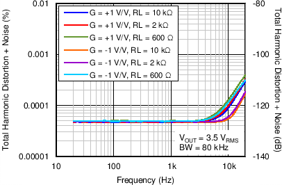
Superior THD Performance

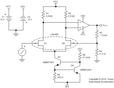
JFET-Input Low-Noise Amplifier
