SBOS391B December 2007 – March 2016 OPA454
PRODUCTION DATA.
- 1 Features
- 2 Applications
- 3 Description
- 4 Revision History
- 5 Device Comparison Table
- 6 Pin Configuration and Functions
- 7 Specifications
- 8 Parameter Measurement Information
- 9 Detailed Description
- 10Application and Implementation
- 11Power Supply Recommendations
- 12Layout
- 13Device and Documentation Support
- 14Mechanical, Packaging, and Orderable Information
Package Options
Mechanical Data (Package|Pins)
- DDA|8
Thermal pad, mechanical data (Package|Pins)
- DDA|8
Orderable Information
9 Detailed Description
9.1 Overview
The OPA454 is a low-cost operational amplifier (op amp) with high voltage (100 V) and a relatively high current drive of 50 mA. This device is unity-gain stable and features a gain-bandwidth product of 2.5 MHz. The high-voltage OPA454 offers excellent accuracy, wide output swing, and has no phase inversion problems that are typically found in similar op amps. The device can be used in virtually any ±5-V to ±50-V op amp configuration, and is especially useful for supply voltages greater than 36 V.
9.2 Functional Block Diagram
9.3 Feature Description
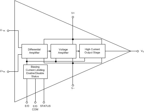
The OPA454 includes safety features on both the device input and output. On the input, protection is provided for a variety of fault conditions. On the output, current limiting and thermal protection are provided. Performance advantages include a ±50-mA output current capability along with the ability to swing to within 1 V of the supply rails. The Enable/Disable function provides the ability to turn off the output stage and reduce power consumption when not being used. The Status Flag indicates fault conditions and can be used in conjunction with the Enable/Disable function to implement fault control loops.
9.3.1 Input Protection
The OPA454 has increased protection against damage caused by excessive voltage between op amp input pins or input pin voltages that exceed the power supplies; external series resistance is not needed for protection. Internal series JFETs limit input overload current to a non-destructive 4 mA, even with an input differential voltage as large as 120 V. Additionally, the OPA454 has dielectric isolation between devices and the substrate. Therefore, the amplifier is free from the limitations of junction isolation common to many IC fabrication processes.
9.3.2 Input Range
The OPA454 is specified to give linear operation with input swing to within 2.5 V of either supply. Generally, a gain of +1 is the most demanding configuration. Figure 57 and Figure 58 show output behavior as the input swings to within 0 V of the rail, using the circuit shown in Figure 60. Figure 59 shows the behavior with an input signal that swings beyond the specified input range to within 1 V of the rail, also using the circuit in Figure 60. Notice that the beginning of the phase reversal effect may be reduced by inserting series resistance (RS) in the connection to the positive input. VOUT does not swing all the way to the opposite rail.
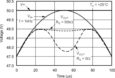 Figure 57. Output Voltage with Input Voltage
 up to V+
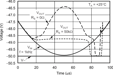 Figure 58. Output Voltage with Input Voltage
 Down to V–
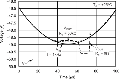 Figure 59. Output Voltage with Input Voltage Down to (V–) + 1 V
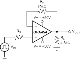 Figure 60. Input Range Test Circuit
9.3.3 Output Range
The OPA454 is specified to swing to within 1 V of either supply rail with a 49-kΩ load while maintaining excellent linearity. Swing to the rail decreases with increasing output current. The OPA454 can swing to within 2 V of the negative rail and 3 V of the positive rail with a 1.88-kΩ load. The typical characteristic curve, Output Voltage Swing vs Output Current (Figure 10), shows this behavior in detail.
9.3.4 Open-Loop Gain Linearity
Figure 61 shows the nonlinear relationship of AOL and output voltage. As Figure 61 shows, open-loop gain is lower with positive output voltage levels compared to negative voltage levels. Specifications in Electrical Characteristics: VS = ±50 V are based upon the average gain measured at both output extremes.
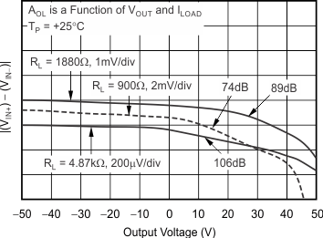 Figure 61. Differential Input Voltage (+IN to –IN) vs Output Voltage
9.3.5 Settling Time
The circuit in Figure 62 is used to measure the settling time response. The left half of the circuit is a standard, false-summing junction test circuit used for settling time and open-loop gain measurement. R1 and R2 provide the gain and allow for measurement without connecting a scope probe directly to the summing junction, which can disturb proper op amp function by causing oscillation.
The right half of the circuit looks at the combination of both inverting and noninverting responses. R5 and R6 remove the large step response. The remaining voltage at V2 shows the small-signal settling time that is centered on zero. This test circuit can be used for incoming inspection, real-time measurement, or in designing compensation circuits in system applications.
Table 1 lists the settling time measurement circuit configuration shown in Figure 62 with different gain settings.
Table 1. Settling Time Measurement Circuit Configuration Using Different Gain Settings for Figure 62
| COMPONENT | GAIN | ||
|---|---|---|---|
| 1 | 5 | 10 | |
| R1 (Ω) | 10 k | 2 k | 1 k |
| R3 (Ω) | 10 k | 2 k | 1 k |
| R7 (Ω) | 10 k | 4 k | 9 k |
| R8 (Ω) | ∞ | 1 k | 1 k |
| VIN (VPP) | 20 | 16 | 8 |
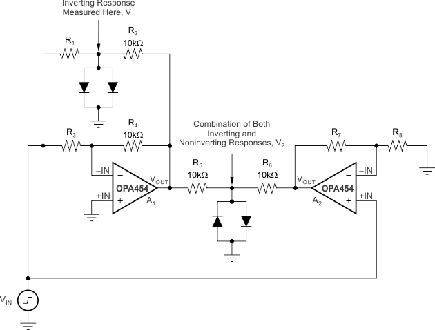 Figure 62. Settling Time Test Measurement Circuit
9.3.6 ENABLE and E/D Com
If left disconnected, E/D Com is pulled near V– (negative supply) by an internal 10-μA current source. When left floating, ENABLE is held approximately 2 V above E/D Com by an internal 1-μA source. Even though active operation of the OPA454 results when the ENABLE and E/D Com pins are not connected, a moderately fast, negative-going signal capacitively coupled to the ENABLE pin can overpower the 1-μA pullup current and cause device shutdown. This behavior can appear as an oscillation and is encountered first near extreme cold temperatures. If the enable function is not used, a conservative approach is to connect ENABLE through a 30-pF capacitor to a low impedance source. Another alternative is the connection of an external current source from V+ (positive supply) sufficient to hold the enable level above the shutdown threshold. Figure 63 shows a circuit that connects ENABLE and E/D Com. Choosing RP to be 1 MΩ with a +50-V positive power supply voltage results in IP = 50 μA.
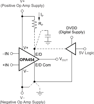 Figure 63. ENABLE and E/D Com
9.3.7 Current Limit
Figure 23 and Figure 47 to Figure 49 show the current limit behavior of the OPA454. Current limiting is accomplished by internally limiting the drive to the output transistors. The output can supply the limited current continuously, unless the die temperature rises to 150°C, which initiates thermal shutdown. With adequate heatsinking, and use of the lowest possible supply voltage, the OPA454 can remain in current limit continuously without entering thermal shutdown. Although qualification studies have shown minimal parametric shifts induced by 1000 hours of thermal shutdown cycling, this mode of operation must be avoided to maximize reliability. It is always best to provide proper heatsinking (either by a physical plate or by airflow) to remain considerably below the thermal shutdown threshold. For longest operational life of the device, keep the junction temperature below 125°C.
9.4 Device Functional Modes
A unique mode of the OPA454 is the output disable capability. This function conserves power during idle periods (quiescent current drops to approximately 150 µA). This disable is accomplished without disturbing the input signal path, not only saving power but also protecting the load. This feature makes disable useful for implementing external fault shutdown loops.