SBOS872A May 2018 – June 2018 OPA521
PRODUCTION DATA.
- 1 Features
- 2 Applications
- 3 Description
- 4 Revision History
- 5 Pin Configuration and Functions
- 6 Specifications
- 7 Detailed Description
- 8 Application and Implementation
- 9 Power Supply Recommendations
- 10Layout
- 11Device and Documentation Support
- 12Mechanical, Packaging, and Orderable Information
Package Options
Mechanical Data (Package|Pins)
- RGW|20
Thermal pad, mechanical data (Package|Pins)
- RGW|20
Orderable Information
9 Power Supply Recommendations
Determining the power-supply requirements requires only a straightforward analysis. The desired load voltage, load impedance, and available power-supply voltage or desired transformer ratio are all the parameters that must be known. In many power-line communication applications, such as PRIME, it is required to drive a 1-VRMS signal into a 2-Ω load. Using Figure 27, calculate the minimum power-supply voltage required by adding the peak-to-peak load voltage; the voltage dropped across the HV Cap and inductor, V2; the voltage dropped across the LV Cap, V1; and twice the output swing to rail limit of the power amplifier, VSWING. For FSK and SFSK systems, the peak to average ratio is √2, while for OFDM systems this ratio is approximately 3:1.
 Figure 27. Typical Line Coupling Circuit
 These ratios must be considered when performing calculations that relate the RMS voltages and peak voltages during an analysis. Choosing a large value for the LV Cap results in the voltage drop (V1) becoming negligible in most circumstances. The losses in the transformer are also negligible, even at high load currents, if the proper transformer with a low DCR is used. For FSK and SFSK systems, the voltage drop across the HV Cap and inductor, V2, is also usually negligible; in OFDM systems, because of the wider operating bandwidth, voltage drop V2 can be ignored and accounted for by using a 1.5× multiplier on the load voltage as an approximation.
NOTE
This approximation is only valid with a load impedance of 2 Ω for PRIME and G3. Voltage drop V2 becomes negligible with increasing load impedance. These assumptions greatly simplify the analysis.
Table 3. Power-Supply Requirements
| PARAMETER | FSK OR SFSK | PRIME OR G3 OFDM | UNIT |
|---|---|---|---|
| Frequency range | 63 to 74 | 35 to 95 | kHz |
| RLOAD | 2 | 2 | Ω |
| VLOAD | 1 | 1 | VRMS |
| VLOAD | 1.414 | 3 | VPEAK |
| VLOAD | 2.828 | 6 | VPP |
| OFDM multiplier | — | 1.5 | — |
| VSWING | 2 | 2 | V |
| Turns ration, N1/N2 | 1.5 | 1.5 | — |
| PA supply | 8.25 | 17.5 | V |
Table 3 summarizes the power-supply requirements for various power-line communication systems.
Example:
For PRIME or G3 using an OFDM signal with a 2-Ω load and 1-VRMSload voltage:
PASupply = VLOAD × OFDM Multiplier × Turns Ration + (2 × VSWING)
PASupply = 6 V × 1.5 × 1.5 + (2 × 2 V)
PASupply = 17.5 V
Power consumption
Calculating the power dissipation in the load and in OPA521 also requires some direct calculations. The desired load voltage, load impedance, available power-supply voltage, and the transformer ratio are the only parameters required. In many power-line communication applications, such as PRIME, it is required to drive a 1-VRMS signal into a 2-Ω load. The power dissipation in the power amplifier is determined by calculating the RMS value of the OPA521’s output current, and the voltage difference between the power amplifier supply and RMS value of the output voltage. These two values are multiplied, and the quiescent power of the power amplifier is added.
The power in the load is given as Equation 4 shows.

The power amplifier output current is given as calculated by Equation 5.

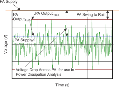
Because the output of the power amplifier is always symmetric around PASupply/2, only the voltage difference between the amplifier supply and the RMS values of the PA output must be considered. Figure 28 illustrates this concept for an OFDM signal. Table 4 shows example power dissipation values.
 Figure 28. Typical OFDM Output Waveforms
 Table 4. Power Dissipation
| PARAMETER | FSK OR SFSK | PRIME OR G3 OFDM | UNITS |
|---|---|---|---|
| Turns ration, N1/N2 | 1.5 | 1.5 | - |
| RLOAD | 2 | 2 | Ω |
| VLOAD | 1 | 1 | VRMS |
| ILOAD | 0.5 | 0.5 | ARMS |
| PA output voltage | 6 | 10.75 | VRMS |
| Voltage drop across PA | 3 | 6.25 | VRMS |
| PA output current | 0.333 | 0.333 | ARMS |
| PA supply | 9 | 17 | V |
| PA power dissipation | 1 | 2.1 | W |
| Load power dissipation | 0.5 | 0.5 | W |
| Total | 1.5 | 2.6 | W |
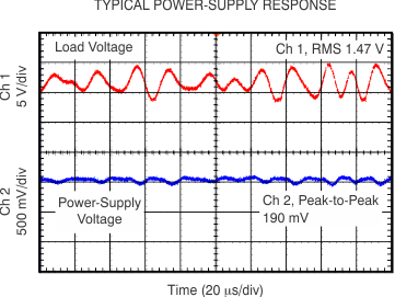
The power supply itself does not need to be designed to supply the peak power amplifier current continuously. The peak demand for current is supplied by the power-supply bypass capacitance. The power-supply voltage is shown in Figure 29 on channel 2, along with the signal voltage at the 2-Ω load on channel 1.
 Figure 29. Typical Power-Supply AC Response
 Two power-supply pins and two ground pins are available to provide a path for the high currents associated with driving the low impedance of the ac mains. Connecting the two supply pins together is recommended. Placing a 47-μF to 100-μF bypass capacitor in parallel with a 100-nF capacitor as close as possible to the device is also recommended. Care must be taken when routing the high-current ground lines on the PCB to avoid creating voltage drops in the PCB ground that may vary with changes in load current. /