SBOS872A May 2018 – June 2018 OPA521
PRODUCTION DATA.
- 1 Features
- 2 Applications
- 3 Description
- 4 Revision History
- 5 Pin Configuration and Functions
- 6 Specifications
- 7 Detailed Description
- 8 Application and Implementation
- 9 Power Supply Recommendations
- 10Layout
- 11Device and Documentation Support
- 12Mechanical, Packaging, and Orderable Information
Package Options
Mechanical Data (Package|Pins)
- RGW|20
Thermal pad, mechanical data (Package|Pins)
- RGW|20
Orderable Information
10.1.1 Thermal Considerations
In a typical power line communications application, the device dissipates 2 W of power when transmitting to the low-impedance AC line. This amount of power dissipation can increase the junction temperature, which can lead to a thermal overload that results in signal transmission interruptions if the PCB thermal design is not implemented properly. Proper management of heat flow from the device and good PCB design and construction are required to ensure proper device temperature, maximize performance, and extend the operating life of the device.
The device is assembled in a 5-mm × 5-mm, QFN-20 package. This QFN package has a large exposed thermal pad on the underside that conducts heat away from the device and to the underlying PCB.
Some heat is conducted from the silicon die surface through the plastic packaging material and is transferred to the ambient environment. However, this route is not the primary thermal path for heat flow because plastic is a relatively poor conductor of heat. Heat flows across the silicon die surface to the bond pads through the wire bonds to the package leads, to the top layer of the PCB. While these paths for heat flow are important, the majority (nearly 80%) of the heat flows downward through the silicon die to the thermally-conductive die-attach epoxy and to the exposed thermal pad on the underside of the package (as shown in Figure 30). Minimizing the thermal resistance of this downward path to the ambient environment maximizes the life and performance of the device.
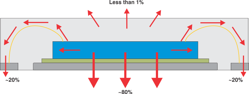 Figure 30. Heat Flow in the QFN Package
 The exposed thermal pad must be soldered to the PCB thermal pad. The thermal pad on the PCB must be the same size as the exposed thermal pad on the underside of the QFN package. See QFN/SON PCB Attachment for recommendations on attaching the thermal pad to the PCB. Figure 31 shows the direction of heat spreading to the PCB from the device.
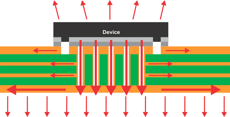 Figure 31. Heat Spreading to PCB
 The heat spreading to the PCB is maximized if the thermal path is uninterrupted. Best results are achieved if the heat-spreading surfaces are filled with copper to the greatest extent possible, which maximizes the percentage of area covered on each layer. As an example, a thermally robust, multilayer PCB design consists of four layers with copper (Cu) coverage of 60% in the top layer, 85% and 90% in the inner layers (respectively), and 95% on the bottom layer.
Increasing the number of layers in the PCB, using thicker copper, and increasing the PCB area are all factors that improve the spread of heat. Figure 32 through Figure 34 show thermal resistance performance as a function of each of these factors.
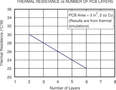 Figure 32. Thermal Resistance as a Function of the Number of Layers in the PCB
 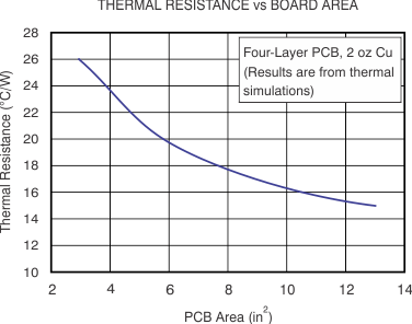 Figure 33. Thermal Resistance as a Function of PCB Area
 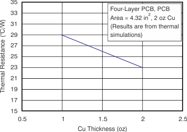 Figure 34. Thermal Resistance as a Function of Copper Thickness
 For additional information on thermal PCB design using exposed thermal pad packages, see PowerPAD™ Thermally-Enhanced Package (available for download at www.ti.com).