SBOS872A May 2018 – June 2018 OPA521
PRODUCTION DATA.
- 1 Features
- 2 Applications
- 3 Description
- 4 Revision History
- 5 Pin Configuration and Functions
- 6 Specifications
- 7 Detailed Description
- 8 Application and Implementation
- 9 Power Supply Recommendations
- 10Layout
- 11Device and Documentation Support
- 12Mechanical, Packaging, and Orderable Information
Package Options
Mechanical Data (Package|Pins)
- RGW|20
Thermal pad, mechanical data (Package|Pins)
- RGW|20
Orderable Information
8.2 Typical Application
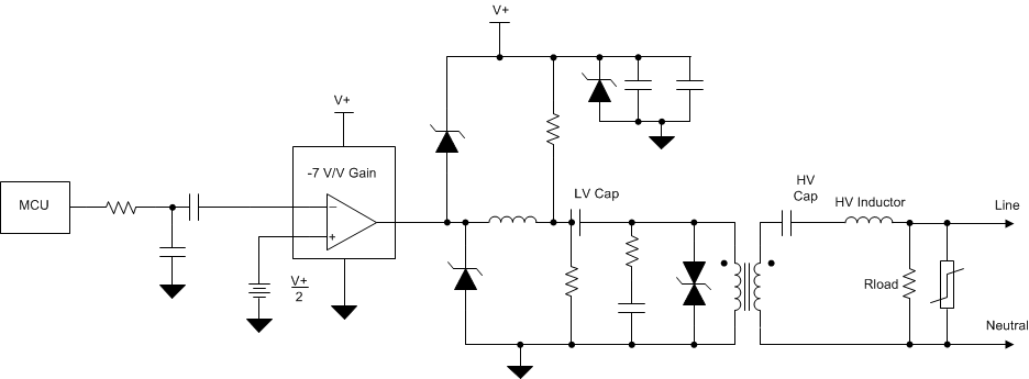
The impedance of the mains network at these signaling frequencies is relatively low (< 1 Ω to 30 Ω). This circuit has been designed to drive a 2-Ω mains line over the 40-kHz-to-90-kHz bandwidth. The signaling impedance of the mains network fluctuates as different loads are switched on during the day or over a season and it is influenced by many factors such as:
- Localized loading from appliances connected to the mains supply near to the connection of the communication equipment; for example, heavy loads such as cookers and immersion heaters and reactive loads such as EMC filters and power factor corrections.
- Distributed loading from consumers connected to the same mains cable, where their collective loading reduces the mains signaling impedance during times of peak electricity consumption; for example, meal times.
- Network parameters; for example, transmission properties of cables and the impedance characteristics of distribution transformers and other system elements.
With such a diversity of factors, the signaling environment fluctuates enormously, irregularly, and can differ greatly from one installation to another. Design the signaling system for reliable communications over a wide range of mains impedances and signaling conditions. Consequently, the transmitter must be able to drive sufficient signal into the mains network under these loading conditions.
The OPA521 amplifier has 1.9-A output drive capability with short-circuit protection; hence, it adequately copes with the high current demands required for implementing mains signaling systems.
 Figure 20. OPA521 Interface to the AC Mains