SBOS153B September   2000  – January 2016 OPA541

PRODUCTION DATA.  

  1. Features
  2. Applications
  3. Description
  4. Revision History
  5. Pin Configuration and Functions
  6. Specifications
    1. 6.1 Absolute Maximum Ratings
    2. 6.2 ESD Ratings
    3. 6.3 Recommended Operating Conditions
    4. 6.4 Thermal Information
    5. 6.5 Electrical Characteristics
    6. 6.6 Typical Characteristics
  7. Detailed Description
    1. 7.1 Overview
    2. 7.2 Functional Block Diagram
    3. 7.3 Feature Description
    4. 7.4 Device Functional Modes
  8. Application and Implementation
    1. 8.1 Application Information
      1. 8.1.1 Current Limit
      2. 8.1.2 Heat Sinking
      3. 8.1.3 Safe Operating Area
      4. 8.1.4 Replacing Hybrid Power Amplifiers
    2. 8.2 Typical Applications
      1. 8.2.1 Clamping Output for EMF-Generating Loads
        1. 8.2.1.1 Design Requirements
        2. 8.2.1.2 Detailed Design Procedure
          1. 8.2.1.2.1 Power Supply Requirements
          2. 8.2.1.2.2 Current Limit and SOA (Safe Operating Area)
          3. 8.2.1.2.3 Heat Sinking
        3. 8.2.1.3 Application Curve
      2. 8.2.2 Paralleled Operation, Extended SOA
        1. 8.2.2.1 Design Requirements
      3. 8.2.3 Programmable Voltage Source
        1. 8.2.3.1 Design Requirements
      4. 8.2.4 16-Bit Programmable Voltage Source
        1. 8.2.4.1 Design Requirements
  9. Power Supply Recommendations
  10. 10Layout
    1. 10.1 Layout Guidelines
    2. 10.2 Layout Example
  11. 11Device and Documentation Support
    1. 11.1 Documentation Support
      1. 11.1.1 Related Documentation
    2. 11.2 Community Resources
    3. 11.3 Trademarks
    4. 11.4 Electrostatic Discharge Caution
    5. 11.5 Glossary
  12. 12Mechanical, Packaging, and Orderable Information

Package Options

Mechanical Data (Package|Pins)
Thermal pad, mechanical data (Package|Pins)
Orderable Information

7 Detailed Description

7.1 Overview

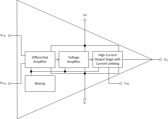
The OPA541 uses a JFET input stage, followed by a main voltage gain stage, and a class A/B high current output stage.

7.2 Functional Block Diagram
OPA541 OPA541_Functional_Block_Diagram_sbos153.gif

7.3 Feature Description

The OPA541 JFET input stage reduces circuit loading and input bias currents. The class A/B high current output stage incorporates temperature compensated biasing to reduce crossover distortion. The output stage also includes a user settable current limit for amplifier and circuit protection.

7.4 Device Functional Modes

The OPA541 has a single functional mode. The OPA541 is operational when the power supply voltage exceeds 10 V (±5 V) and less than 80 V (±40 V).