SBOS100B July 1999 – January 2016 OPA551 , OPA552
PRODUCTION DATA.
- 1 Features
- 2 Applications
- 3 Description
- 4 Revision History
- 5 Pin Configuration and Functions
- 6 Specifications
- 7 Detailed Description
- 8 Application and Implementation
- 9 Power Supply Recommendations
- 10Layout
- 11Device and Documentation Support
- 12Mechanical, Packaging, and Orderable Information
Package Options
Mechanical Data (Package|Pins)
Thermal pad, mechanical data (Package|Pins)
Orderable Information
8 Application and Implementation
NOTE
Information in the following applications sections is not part of the TI component specification, and TI does not warrant its accuracy or completeness. TI’s customers are responsible for determining suitability of components for their purposes. Customers should validate and test their design implementation to confirm system functionality.
8.1 Application Information
Figure 27 shows the OPA551 connected as a basic noninverting amplifier. The OPA551 can be used in virtually any operational amplifier configuration. The OPA552 is designed for use in configurations with gains of 5 or greater. Power-supply terminals must be bypassed with 0.1-µF capacitors, or greater, near the power-supply pins. Be sure that the capacitors are appropriately rated for the power-supply voltage used. The OPA55x can supply output currents up to 200 mA with excellent performance.
8.2 Typical Application
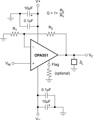 Figure 27. Basic Circuit Connections
8.2.1 Design Requirements
- Operate from power supplies between ±15 V to ±30 V
- Drive passive and reactive loads up to 1 A
- Drive large capacitive loads
- Operate up to 125°C
8.2.2 Detailed Design Procedure
8.2.2.1 Capacitive Loads
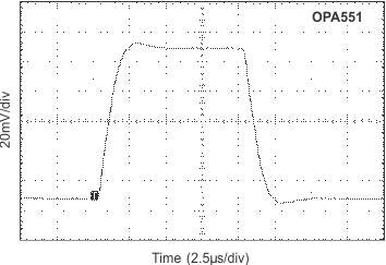
The dynamic characteristics of the OPA55x have been optimized for commonly-encountered gains, loads, and operating conditions. The combination of low closed-loop gain and capacitive load decreases the phase margin and may lead to gain peaking or oscillations. Figure 28 shows a circuit that preserves phase margin with a 10-nF capacitive load. Figure 33 shows the small-signal step response for the circuit in Figure 28. Consult SBOA015 for more information.
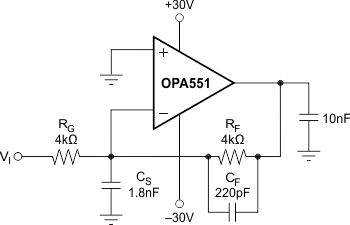 Figure 28. Driving Large Capacitive Loads
8.2.2.2 Increasing Output Current
In those applications where the 200 mA of output current is not sufficient to drive the desired load, output current can increase by connecting two or more OPA551s or OPA552s in parallel, as shown in Figure 29. Amplifier A1 is the master amplifier and may be configured in virtually an operational amplifier circuit. Amplifier A2, the slave, is configured as a unity-gain buffer. Alternatively, external output transistors can be used to boost output current. The circuit in Figure 30 is capable of supplying output currents up to 1 A. Alternatively, consider the OPA547, OPA548, and OPA549 series power operational amplifiers for high output current drive, along with programmable current limit and output disable capability.
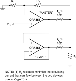 Figure 29. Parallel Amplifiers Increase Output Current Capability
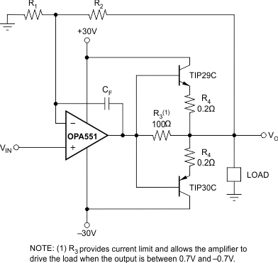 Figure 30. External Output Transistors Boost Output Current Up to 1 A
8.2.2.3 Using the OPA552 in Low Gains
The OPA552 family is intended for applications with signal gains of 5 or greater, but it is possible to take advantage of the high slew rate in lower gains using an external compensation technique in an inverting configuration. This technique maintains low-noise characteristics of the OPA552 architecture at low frequencies. Depending on the application, a small increase in high-frequency noise may result. This technique shapes the loop gain for good stability while giving an easily-controlled, second-order, lowpass frequency response.
Considering only the noise gain (noninverting signal gain) for the circuit of Figure 31, the low-frequency noise gain (NG1) is set by the resistor ratios, while the high-frequency noise gain (NG2) is set by the capacitor ratios. The capacitor values set both the transition frequencies and the high-frequency noise gain. If this noise gain, determined by NG2 = 1 + CS / CF, is set to a value greater than the recommended minimum stable gain for the operational amplifier and the noise gain pole, set by 1 / RFCF, is placed correctly, a very well-controlled, second-order, lowpass frequency response is the result.
To choose the values for both CS and CF, two parameters and only three equations must be solved. First, the target for the high-frequency noise gain (NG2) must be greater than the minimum stable gain for the OPA552. In the circuit shown in Figure 31, a target NG2 of 10 is used. Second, the signal gain of –1 shown in Figure 31 sets the low frequency noise gain to NG1 = 1 + RF / RG (= 2 in this example). Using these two gains, knowing the gain bandwidth product (GBP) for the OPA552 (12 MHz), and targeting a maximally flat, second-order, lowpass Butterworth frequency response (Q = 0.707), the key frequency in the compensation can be found.
For the values shown in Figure 31, the f–3dB is approximately 956 kHz. This frequency is less than that predicted by simply dividing the GBP by NG1. The compensation network controls the bandwidth to a lower value while providing the full slew rate at the output and an exceptional distortion performance as a result of increased loop gain at frequencies below NG1 × Z0. The capacitor values shown in Figure 31 are calculated for NG1 = 2 and NG2 = 10 with no adjustment for parasitics.
Optimize the actual circuit values by checking the small-signal step response with actual load conditions. Figure 32 shows the small-signal step response of this OPA552, G = –1 circuit with a 500-pF load. It is well-behaved with no tendency to oscillate. If CS and CF are removed, the circuit becomes unstable.
SPACER
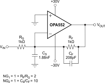 Figure 31. Compensation of the OPA552 for G = 1
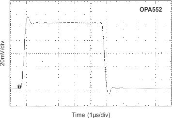 Figure 32. Small-Signal Step Response for Figure 31
8.2.2.4 Offset Voltage Error Calculation
The offset voltage (VOS) of the OPA51 and OPA552 is specified with a ±30-V power supply and the common-mode voltage centered between the supplies (VS / 2 = 0 V). Additional specifications for power-supply rejection and common-mode rejection are provided to allow the user to easily calculate worst-case excepted offset under the conditions of a given application.
Power-supply rejection ratio (PSRR) is specified in µV/V. For the OPA55x, worst-case PSRR is 30 µV/V, which means for each volt of change in total power-supply voltage, the offset may shift by up to 30 µV/V. Common-mode rejection ratio (CMRR) is specified in dB, which can be converted to µV/V using Equation 1:
For the OPA55x, the worst-case CMRR at ±30-mV supply over the full common-mode range is 96 dB, or approximately 15.8 µV/V. This result means that for every volt of change in common-mode, the offset may shift up to 15.8 µV. These numbers can be used to calculate excursions from the specified offset voltage under different applications conditions. For example, a common application might configure the amplifier with a –48-V single supply with –6-V common-mode. This configuration represents a 12-V variation in power supply: ±30 V or 60 V in the offset specification versus 48 V in the application. In addition, this configuration has an 18-V variation in common-mode voltage: VS / 2 = –24 V is the specification for these power supplies, but the common-mode voltage is –6 V in the application.
Calculation of the worst-case expected offset for this example is calculated by Equation 2 and Equation 3.
