SBOS100B July 1999 – January 2016 OPA551 , OPA552
PRODUCTION DATA.
- 1 Features
- 2 Applications
- 3 Description
- 4 Revision History
- 5 Pin Configuration and Functions
- 6 Specifications
- 7 Detailed Description
- 8 Application and Implementation
- 9 Power Supply Recommendations
- 10Layout
- 11Device and Documentation Support
- 12Mechanical, Packaging, and Orderable Information
Package Options
Mechanical Data (Package|Pins)
Thermal pad, mechanical data (Package|Pins)
Orderable Information
10 Layout
10.1 Layout Guidelines
The circuit board must have as much ground plane area as possible. Power supply and output traces must be sized to handle the required current. Keep input and output terminals separated as much as possible.
10.2 Layout Example
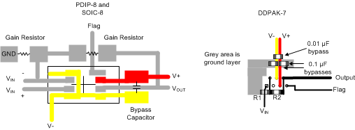 Figure 34. Layout Example (OPA551)
10.3 Power Dissipation
Internal power dissipation of these operational amplifiers can be quite large. Many of the specifications for the OPA55x are for a specified junction temperature. If the device is not subjected to internal self-heating, the junction temperature is the same as the ambient. However, in practical applications, the device self-heats and the junction temperature becomes significantly higher than ambient. After junction temperature has been established, performance parameters that vary with junction temperature can be determined from the performance curves. The following calculation can be performed to establish junction temperature as a function of ambient temperature and the conditions of the application.
Consider the OPA551 in a circuit configuration where the load is 600 Ω and the output voltage is 15 V. The supplies are at ±30 V and the ambient temperature (TA) is 40°C. The θJA for the 8-pin PDIP package is 100°C/W.
First, the internal heating of the operational amplifier is in Equation 4:
The output current (IO) can be calculated in Equation 5:
The power being dissipated (PD) in the output transistor of the amplifier can be calculated in Equation 6 and Equation 7:
The resulting junction temperature can be calculated in Equation 8 and Equation 9:
where
- TJ = junction temperature (°C)
- TA = ambient temperature (°C)
- θJA = junction-to-air thermal resistance (°C/W)
For the DDPAK/TO-263 package, the θJA is 65°C/W with no heat sinking, resulting in a junction temperature of 92.5°C.
To estimate the margin of safety in a complete design (including heatsink), increase the ambient temperature until the thermal protection is activated. Use worst-case load and signal conditions. For good reliability, the thermal protection must trigger more than 35°C above the maximum expected ambient condition of a given application. This limit ensures a maximum junction temperature of 125°C at the maximum expected ambient condition.
If the OPA551 or OPA552 is to be used in an application requiring more than 0.5-W continuous power dissipation, TI recommends that the DDPAK/TO-263 package option be used. The DDPAK/TO-263 has superior thermal dissipation characteristics and is more easily adapted to a heatsink.
Operation from a single power supply (or unbalanced power supplies) can produce even larger power dissipation because a larger voltage can be impressed across the conducting output transistor. Consult SBOA022 for further information on how to calculate or measure power dissipation.
Power dissipation can be minimized by using the lowest possible supply voltage. For example, with a 200-mA load, the output swings to within 3.5 V of the power-supply rails. Set the power supplies to no more than 3.5 V above the maximum output voltage swing required by the application to minimize the power dissipation.
10.4 Safe Operating Area
The Safe Operating Area (SOA) curves Figure 35, Figure 36, and Figure 37 show the permissible range of voltage and current. These curves shown represent devices soldered to a circuit board with no heatsink. The safe output current decreases as the voltage across the output transistor (VS – VO) increases. For further insight on SOA, consult AB-039.
Output short circuits are a very demanding case for SOA. A short-circuit to ground forces the full power-supply voltage (V+ or V–) across the conducting transistor and produces a typical output current of 380 mA. With ±30-V power supplies, this configuration creates an internal dissipation of 11.4 W. This dissipation far exceeds the maximum rating and is not recommended. If operation in this region is unavoidable, use the DDPAK/TO-263 package with a heatsink.
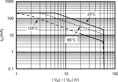 Figure 35. PDIP-8 Safe Operating Area
 Figure 36. SOIC-8 Safe Operating Area
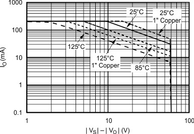 Figure 37. DDPAK-7/TO-263 Safe Operating Area
10.5 Heat Sinking
Power dissipated in the OPA551 or OPA552 causes the junction temperature to rise. For reliable operation, limit the junction temperature to 125°C. Many applications require a heatsink to assure that the maximum operating junction temperature is not exceeded. The heatsink required depends on the power dissipated and on ambient conditions.
For heatsinking purposes, the tab of the DDPAK/TO-263 is typically soldered directly to the PCB copper area. Increasing the copper area improves heat dissipation. Figure 38 shows typical thermal resistance from junction-to-ambient as a function of copper area.
Depending on conditions, additional heatsinking may be required. Aavid Thermal Products Inc. manufactures surface-mountable heatsinks designed specifically for use with DDPAK/TO-263 packages. Further information is available on the Aavid web site, www.aavid.com.
To estimate the margin of safety in a complete design (including heatsink), increase the ambient temperature until the thermal protection is activated. Use worst-case load and signal conditions. For good reliability, the thermal protection must trigger more than 25°C above the maximum expected ambient condition of your application. This level produces a junction temperature of 125°C at the maximum expected ambient condition.
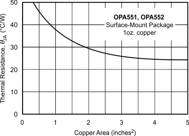 Figure 38. Thermal Resistance vs Circuit Board Copper Area
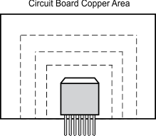 Figure 39. OPA551, OPA552 Surface-Mount Package Circuit Board Copper Area