SBOS688A April 2015 – October 2015 OPA2625 , OPA625
PRODUCTION DATA.
- 1 Features
- 2 Applications
- 3 Description
- 4 Revision History
- 5 Pin Configuration and Functions
-
6 Specifications
- 6.1 Absolute Maximum Ratings
- 6.2 ESD Ratings
- 6.3 Recommended Operating Conditions
- 6.4 Thermal Information
- 6.5 Electrical Characteristics High-Drive Mode
- 6.6 Electrical Characteristics Low-Power Mode
- 6.7 Electrical Characteristics High-Drive Mode
- 6.8 Electrical Characteristics Low-Power Mode
- 6.9 Switching Characteristics
- 6.10 Typical Characteristics
- 7 Parameter Measurement Information
- 8 Detailed Description
- 9 Application and Implementation
- 10Power Supply Recommendations
- 11Layout
- 12Device and Documentation Support
- 13Mechanical, Packaging, and Orderable Information
Package Options
Mechanical Data (Package|Pins)
- DBV|6
Thermal pad, mechanical data (Package|Pins)
Orderable Information
6 Specifications
6.1 Absolute Maximum Ratings
over operating free-air temperature range (unless otherwise noted)(1)| MIN | MAX | UNIT | ||
|---|---|---|---|---|
| Supply voltage, VS | (V+) – (V–) | 6 | V | |
| Input voltage(2) | +IN | (V–) – 0.3 | (V+) + 0.3 | V |
| –IN | (V–) – 0.3 | (V+) + 0.3 | ||
| MODE | (V–) – 0.3 | (V+) + 0.3 | ||
| Output voltage | OUT | (V–) | (V+) | V |
| Sink current | +IN | 10 | mA | |
| –IN | 10 | |||
| MODE | 10 | |||
| OUT | 150 | |||
| Source current | +IN | 10 | mA | |
| –IN | 10 | |||
| MODE | 10 | |||
| OUT(2) | 150 | |||
| Temperature | Operating junction | –40 | 150 | °C |
| Storage, Tstg | –65 | 150 | ||
(1) Stresses beyond those listed under Absolute Maximum Ratings may cause permanent damage to the device. These are stress ratings only, which do not imply functional operation of the device at these or any other conditions beyond those indicated under Recommended Operating Conditions. Exposure to absolute-maximum-rated conditions for extended periods may affect device reliability.
(2) For input voltages beyond the power-supply rails, voltage or current must be limited.
6.2 ESD Ratings
| VALUE | UNIT | |||
|---|---|---|---|---|
| V(ESD) | Electrostatic discharge | Human-body model (HBM), per ANSI/ESDA/JEDEC JS-001(1) | ±3000 | V |
| Charged-device model (CDM), per JEDEC specification JESD22-C101(2) | ±1500 | |||
(1) JEDEC document JEP155 states that 500-V HBM allows safe manufacturing with a standard ESD control process.
(2) JEDEC document JEP157 states that 250-V CDM allows safe manufacturing with a standard ESD control process.
6.3 Recommended Operating Conditions
over operating free-air temperature range (unless otherwise noted)| MIN | NOM | MAX | UNIT | |||
|---|---|---|---|---|---|---|
| VS | Supply input voltage, (V+) – (V–) | 2.7 | 5.5 | V | ||
| VI | Input voltage | +IN | (V–) | (V+) – 1.15 | V | |
| –IN | (V–) | (V+) – 1.15 | ||||
| MODE | (V–) | (V+) | ||||
| VO | Output voltage | (V–) | (V+) | V | ||
| IO | Output current | –120 | 120 | mA | ||
| TA | Operating free-air temperature | –40 | 125 | °C | ||
| TJ | Operating junction temperature | –40 | 125 | °C | ||
6.4 Thermal Information
| THERMAL METRIC(1) | OPA625 | OPA2625 | UNIT | |
|---|---|---|---|---|
| DBV (SOT) | DGS (VSSOP) | |||
| 6 PINS | 10 PINS | |||
| RθJA | Junction-to-ambient thermal resistance | 184.9 | 171.7 | °C/W |
| RθJC(top) | Junction-to-case (top) thermal resistance | 123.6 | 68.4 | °C/W |
| RθJB | Junction-to-board thermal resistance | 30.7 | 91.9 | °C/W |
| ψJT | Junction-to-top characterization parameter | 22.1 | 9.4 | °C/W |
| ψJB | Junction-to-board characterization parameter | 30.2 | 90.5 | °C/W |
| RθJC(bot) | Junction-to-case (bottom) thermal resistance | N/A | N/A | °C/W |
(1) For more information about traditional and new thermal metrics, see the Semiconductor and IC Package Thermal Metrics application report, SPRA953.
6.5 Electrical Characteristics High-Drive Mode
at TA = 25°C, V+ = 5 V, V– = 0 V, MODE pin connected to V– pin, VCOM = VO = 2.5 V, gain (G) = 1, RF = 1 kΩ, CF = 2.7 pF, CLOAD = 20 pF, and RLOAD = 2 kΩ connected to 2.5 V (unless otherwise noted)| PARAMETER | TEST CONDITIONS | MIN | TYP | MAX | UNIT | ||
|---|---|---|---|---|---|---|---|
| AC PERFORMANCE | |||||||
| Unity gain frequency | VO = 10 mVPP | 80 | MHz | ||||
| φm | Phase margin | 50 | Degrees | ||||
| GBW | Gain-bandwidth product | G = 100, VO = 10 mVPP | 120 | MHz | |||
| SR | Slew rate | VO = 1-V step, G = 1 | 45 | V/µs | |||
| VO = 4-V step, G = 2 | 115 | ||||||
| tsettle | Settling time | VO = 4-V step, G = 2 | Settling time to 0.1% (10-bit accuracy) |
80 | ns | ||
| to 0.005% (14-bit accuracy) |
110 | ||||||
| to 0.00153% (16-bit accuracy) |
280 | ||||||
| Overshoot | VO = 4-V step, G = 2 | 2.5% | |||||
| Undershoot | VO = 4-V step, G = 2 | 3% | |||||
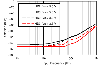
| HD2 | Second-order harmonic Distortion | VO = 2 VPP, G = 2 | f = 10 kHz | 144 | dBc | ||
| f = 100 kHz | 122 | ||||||
| f = 1 MHz | 80 | ||||||
| HD3 | Third-order harmonic Distortion | VO = 2 VPP, G = 2 | f = 10 kHz | 155 | dBc | ||
| f = 100 kHz | 140 | ||||||
| f = 1 MHz | 80 | ||||||
| Second-order intermodulation distortion | VO = 2 VPP, f = 1 MHz, 200-kHz tone spacing | 90 | dBc | ||||
| Third-order intermodulation distortion | VO = 2 VPP, f = 1 MHz, 200-kHz tone spacing | 100 | dBc | ||||
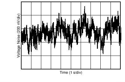
| VN | Input noise voltage | f = 0.1 Hz to 10 Hz, peak-to-peak | 0.8 | µVPP | |||
| f = 0.1 Hz to 10 Hz, rms | 120 | nVRMS | |||||
| Vn | Input voltage noise density | f = 1 kHz | 3.2 | nV/√Hz | |||
| f = 10 kHz | 2.5 | ||||||
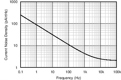
| In | Input current noise density | f = 1 kHz | 4.1 | pA/√Hz | |||
| f = 10 kHz | 2.8 | ||||||
| tOR | Overload recovery time | G = 5 | 50 | ns | |||
| Zo | Open-loop output impedance | f = 1 MHz | 1 | Ω | |||
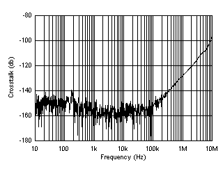
| Crosstalk | DC | 150 | dB | ||||
| f = 1 MHz | 127 | ||||||
| DC PERFORMANCE | |||||||
| VOS | Input offset voltage | 15 | ±100 | µV | |||
| TA = –40°C to +125°C | ±300 | ||||||
| dVOS/dT | Input offset voltage drift | TA = –40°C to +125°C | 0.5 | ±3 | µV/°C | ||
| OPA2625 only, TA = –40°C to +125°C | 0.6 | ±4 | |||||
| PSRR | Power-supply rejection ratio | 2.7 V ≤ (V+) ≤ 5 V | 100 | dB | |||
| TA = –40°C to +125°C | 90 | 120 | |||||
| IB | Input bias current | 2 | 4 | µA | |||
| TA = –40°C to +125°C | 5.7 | ||||||
| OPA2625 only, TA = –40°C to +125°C | 6.5 | ||||||
| dIB/dT | Input bias current drift | TA = –40°C to +125°C | 15 | nA/°C | |||
| IOS | Input offset current | 20 | 120 | nA | |||
| TA = –40°C to +125°C | 150 | ||||||
| OPA2625 only, TA = –40°C to +125°C | 200 | ||||||
| dIOS/dT | Input offset current drift | TA = –40°C to +125°C | 0.6 | nA/°C | |||
| OPEN LOOP GAIN | |||||||
| AOL | Open-loop gain | (V–) + 0.2 V < VO < (V+) – 0.2 V, RLOAD = 600 Ω | 110 | dB | |||
| (V–) + 0.15 V < VO < (V+) – 0.15 V, RLOAD = 10 kΩ | 114 | ||||||
| TA = –40°C to +125°C | (V–) + 0.2 V < VO < (V+) – 0.2 V, RLOAD = 600 Ω |
106 | 128 | ||||
| (V–) + 0.15 V < VO < (V+) – 0.15 V, RLOAD = 10 kΩ |
110 | 132 | |||||
| INPUT VOLTAGE | |||||||
| VCM | Common-mode voltage range | TA = –40°C to +125°C | (V–) | (V+) – 1.15 | V | ||
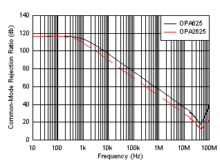
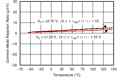
| CMRR | Common-mode rejection ratio | (V–) < VCOM < (V+) – 1.15 V | 100 | 117 | dB | ||
| TA = –40°C to +125°C | 90 | 115 | |||||
| INPUT IMPEDANCE | |||||||
| ZID | Differential input impedance | 27 || 1.2 | KΩ || pF | ||||
| ZIC | Common-mode input impedance | 47 || 1.5 | MΩ || pF | ||||
| OUTPUT | |||||||
| Output voltage swing to the rail | RLOAD = 600 Ω | 60 | 80 | mV | |||
| TA = –40°C to +125°C | 100 | ||||||
| RLOAD = 10 kΩ | 20 | 35 | |||||
| TA = –40°C to +125°C | 40 | ||||||
| Isc | Short-circuit current | 150 | mA | ||||
| CLOAD | Capacitive load drive | See Typical Characteristics | |||||
| MODE | |||||||
| VIL | High-drive (HD) mode threshold | TA = –40°C to +125°C | (V–) | (V–) + 0.5 | V | ||
| VIH | Low-power (LP) mode threshold | TA = –40°C to +125°C | (V–) + 1.2 | (V+) | V | ||
| IIL | Low-level input current | TA = –40°C to +125°C, VMODE ≤ (V–) + 0.5 V | 0.01 | 1 | µA | ||
| IIH | High-level input current | TA = –40°C to +125°C, VMODE ≥ (V–) + 1.2 V | 20 | 30 | µA | ||
| OPA2625 only, TA = –40°C to +125°C, VMODE ≥ (V–) + 1.2 V | 1 | ||||||
| POWER SUPPLY | |||||||
| IQ | Quiescent current per amplifier | IO = 0 mA, MODE connected to ground |
2 | 2.2 | mA | ||
| TA = –40°C to +125°C | 3.1 | ||||||
6.6 Electrical Characteristics Low-Power Mode
at TA = 25°C, V+ = 5 V, V– = 0 V, VMODE = 5 V, VCOM = VO = 2.5 V, gain (G) = 1, RF = 1 kΩ, CF = 2.7 pF, CLOAD = 20 pF, and RLOAD = 2 kΩ connected to 2.5 V (unless otherwise noted)| PARAMETER | TEST CONDITIONS | MIN | TYP | MAX | UNIT | ||
|---|---|---|---|---|---|---|---|
| AC PERFORMANCE | |||||||
| GBW | Gain-bandwidth product | G = 100, VO = 10 mVPP | 1 | MHz | |||
| φm | Phase margin | 72 | Degrees | ||||
| SR | Slew rate | VO = 1-V step | 4.3 | V/µs | |||
| VO = 4-V step, G = 2 | 4.1 | ||||||
| Zo | Open-loop output impedance | f = 1 MHz | 12 | Ω | |||
| DC PERFORMANCE | |||||||
| VOS | Input offset voltage | 0.6 | 3 | mV | |||
| TA = –40°C to +125°C | 0.7 | 3.7 | |||||
| PSRR | Power-supply rejection ratio | 2.7 V ≤ (V+) ≤ 5 V | 74 | dB | |||
| TA = –40°C to +125°C | 70 | 100 | |||||
| IB | Input bias current | 150 | nA | ||||
| TA = –40°C to +125°C | 140 | 200 | |||||
| OPA2625 only, TA = –40°C to +125°C | 250 | ||||||
| IOS | Input offset current | 20 | nA | ||||
| TA = –40°C to +125°C | 25 | ||||||
| OPEN LOOP GAIN | |||||||
| AOL | Open-loop gain | TA = –40°C to +125°C | (V–) + 0.2 V < VO < (V+) – 0.2 V, RLOAD = 600 Ω |
70 | 100 | dB | |
| (V–) + 0.15 V < VO < (V+) – 0.15 V, RLOAD = 10 kΩ |
90 | 100 | |||||
| INPUT VOLTAGE | |||||||
| VCM | Common-mode voltage range | TA = –40°C to +125°C | (V–) | (V+) – 1.15 | V | ||
| CMRR | Common-mode rejection ratio | (V–) < VCOM < (V+) – 1.15 V | 66 | 114 | dB | ||
| TA = –40°C to +125°C | 60 | 114 | |||||
| OUTPUT | |||||||
| Output voltage swing to the rail | TA = –40°C to +125°C | RLOAD = 600 Ω | 110 | mV | |||
| RLOAD = 10 kΩ | 40 | ||||||
| Isc | Short-circuit current | 100 | mA | ||||
| POWER SUPPLY | |||||||
| IQ | Quiescent current per amplifier | IO = 0 mA, MODE connected to V+ |
270 | 320 | µA | ||
| TA = –40°C to +125°C | 450 | ||||||
6.7 Electrical Characteristics High-Drive Mode
at TA = +25°C, V+ = 2.7 V, V– = 0 V, VMODE = 0 V, VCOM = VO = 1.35 V, gain (G) = 1, RF = 1 kΩ, CF = 2.7 pF, CLOAD = 20 pF, and RLOAD = 1 kΩ connected to 1.35 V (unless otherwise noted)| PARAMETER | TEST CONDITIONS | MIN | TYP | MAX | UNIT | ||
|---|---|---|---|---|---|---|---|
| AC PERFORMANCE | |||||||
| Unity gain frequency | VO = 10 mVPP | 76 | MHz | ||||
| φm | Phase margin | 45 | Degrees | ||||
| GBW | Gain-bandwidth product | G = 100, VO = 10 mVPP | 120 | MHz | |||
| SR | Slew rate | VO = 1-V step, G = 2 | 45 | V/µs | |||
| tsettle | Settling time | VO = 1-V step, G = 2 | to 0.1% | 80 | ns | ||
| to 0.01% | 170 | ||||||
| to 0.000763% (17-bit accuracy) | 250 | ||||||
| Overshoot | VO = 1-V step, G = 2 | 6% | |||||
| Undershoot | VO = 1-V step, G = 2 | 5% | |||||
| HD2 | Second order harmonic Distortion | (V+) = 3.3 V, (V–) = 0 V, VCOM = 1.1 V, VO = 2 VPP |
f = 10 kHz | 136 | dBc | ||
| f = 100 kHz | 118 | ||||||
| f = 1 MHz | 80 | ||||||
| HD3 | Third order harmonic Distortion | (V+) = 3.3 V, (V–) = 0 V, VCOM = 1.1 V, VO = 2 VPP |
f = 10 kHz | 143 | dBc | ||
| OPA2625 only, f = 10 kHz | 143 | ||||||
| f = 100 kHz | 130 | ||||||
| OPA2625 only, f = 100 kHz | 125 | ||||||
| f = 1 MHz | 85 | ||||||
| OPA2625 only, f = 1 MHz | 74 | ||||||
| Second order inter-modulation distortion | (V+) = 3.3 V, (V–) = 0 V, VCOM = 1.1 V, VO = 2 VPP, f = 1 MHz, 200-kHz tone spacing |
95 | dBc | ||||
| Third order inter-modulation distortion | (V+) = 3.3 V, (V–) = 0 V, VCOM = 1.1V, VO = 1 VPP, f = 1 MHz, 200-kHz tone spacing |
104 | dBc | ||||
| VN | Input noise voltage | f = 0.1 Hz to 10 Hz peak to peak | 0.8 | µVPP | |||
| f = 0.1 Hz to 10 Hz rms | 120 | nVRMS | |||||
| Vn | Input voltage noise density | f = 10 kHz | 2.5 | nV/√Hz | |||
| In | Input current noise density | f = 10 kHz | 2.8 | pA/√Hz | |||
| tOR | Overload recovery time | G = 5 | 35 | ns | |||
| Zo | Open-loop output impedance | f = 1 MHz | 1.3 | Ω | |||
| Crosstalk | DC | 150 | dB | ||||
| f = 1 MHz | 127 | ||||||
| DC PERFORMANCE | |||||||
| VOS | Input offset voltage | 15 | ±100 | µV | |||
| TA = –40°C to +125°C | ±300 | ||||||
| dVOS/dT | Input offset voltage drift | TA = –40°C to +125°C | 0.5 | ±3.1 | µV/°C | ||
| OPA2625 only, TA = –40°C to +125°C | 0.6 | ±4 | |||||
| IB | Input bias current | 2 | 4 | µA | |||
| TA = –40°C to +125°C | 5.7 | ||||||
| OPA2625 only, TA = –40°C to +125° | 6.5 | ||||||
| dIB/dT | Input bias current drift | TA = –40°C to +125°C | 15 | nA/°C | |||
| IOS | Input offset current | 20 | 120 | nA | |||
| TA = –40°C to +125°C | 150 | ||||||
| OPA2625 only, TA = –40°C to +125° | 200 | ||||||
| dIOS/dT | Input offset current drift | TA = –40°C to +125°C | 80 | pA/°C | |||
| OPEN-LOOP GAIN | |||||||
| AOL | Open-loop gain | (V–) + 0.2 V < VO < (V+) – 0.2 V, RLOAD = 600 Ω |
110 | dB | |||
| (V–) + 0.15 V < VO < (V+) – 0.15 V, RLOAD = 10 kΩ |
114 | ||||||
| TA = –40°C to +125°C | (V–) + 0.2 V < VO < (V+) – 0.2 V, RLOAD = 600 Ω |
106 | 128 | ||||
| (V–) + 0.15 V < VO < (V+) – 0.15 V, RLOAD = 10 kΩ |
110 | 132 | |||||
| INPUT VOLTAGE | |||||||
| VCM | Common-mode voltage range | TA = –40°C to +125°C | (V–) | (V+) – 1.15 | V | ||
| CMRR | Common-mode rejection ratio | (V–) < VCOM < (V+) – 1.15 V | 100 | 117 | dB | ||
| TA = –40°C to +125°C | 90 | 115 | |||||
| INPUT IMPEDANCE | |||||||
| ZID | Differential input impedance | 27 || 0.8 | KΩ || pF | ||||
| ZIC | Common-mode input impedance | 47 || 1.2 | MΩ || pF | ||||
| OUTPUT | |||||||
| Output voltage swing to the rail | R LOAD = 600 Ω | 60 | 80 | mV | |||
| TA = –40°C to +125°C | 100 | ||||||
| R LOAD = 10 kΩ | 20 | 35 | |||||
| TA = –40°C to +125°C | 40 | ||||||
| ISC | Short-circuit current | 80 | mA | ||||
| CLOAD | Capacitive load drive | See Typical Characteristics | |||||
| MODE | |||||||
| VIL | High-drive (HD) mode threshold | TA = –40°C to +125°C | (V–) | (V–) + 0.5 | V | ||
| VIH | Low-power (LP) mode threshold | TA = –40°C to +125°C | (V–) + 1.2 | (V+) | V | ||
| POWER SUPPLY | |||||||
| IQ | Quiescent current per amplifier | IO = 0 mA MODE connected to ground |
2 | 2.1 | mA | ||
| TA = –40°C to +125°C | 2.8 | ||||||
6.8 Electrical Characteristics Low-Power Mode
at TA = +25°C, V+ = 2.7 V, V– = 0 V, VMODE = 2.7 V, VCOM = VO = 1.35V, gain (G) = 1, RF = 1 kΩ, CF = 2.7 pF, CLOAD = 20 pF, and RLOAD = 1 kΩ connected to 1.35 V (unless otherwise noted)6.9 Switching Characteristics
at TA = 25°C, V+ = 5 V, V– = 0 V, MODE pin connected to V– pin, gain (G) = 1 , VCOM = VO = 2.5 V, CLOAD = 20 pF, and RLOAD = 1 kΩ connected to 2.5 V (unless otherwise noted)| PARAMETER | TEST CONDITIONS | MIN | TYP | MAX | UNIT | |
|---|---|---|---|---|---|---|
| tLP-HD | Delay time, MODE pin falling (low-power mode to high-drive mode) |
Settling time to within 50 µV of final value, MODE pin = high to low (LP to HD), VO = 3.8 V |
180 | ns | ||
| tLP-HD is defined as the time taken for the quiescent current to increase from 110% of its value in LP mode to 90% of its value in HD mode. | 170 | ns | ||||
| tHD-LP | Delay time, MODE pin rising (high-drive mode to low-power mode) |
tHD-LP is defined as the time taken for the quiescent current to decrease from 90% of its value in HD mode to 110% of its value in LP mode. | 300 | ns | ||
 Figure 1. Switching Characteristics Timing Diagram
6.10 Typical Characteristics
At TA = 25°C, V+ = 5 V, V– = 0 V, MODE = V–, VCOM = VO = 2.5 V, gain (G) = 2, RF = 1 kΩ, CF= 2.7 pF, CLOAD= 20 pF, and RLOAD = 2 kΩ connected to 2.5 V (unless otherwise noted)
| VO = 10 mVPP |
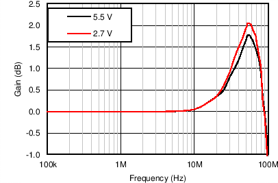
| VO = 10 mVPP, G = 1 |
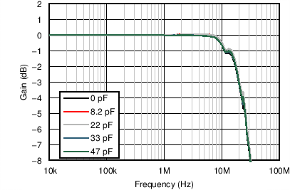
| VO = 2 VPP, G = 1 |
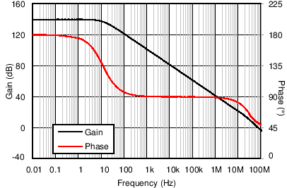
| VO = 10 mVPP |
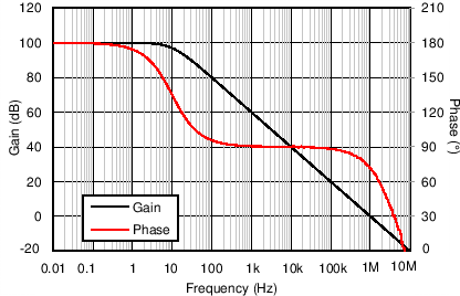
| VO = 10 mVPP , VMODE = 5 V | ||
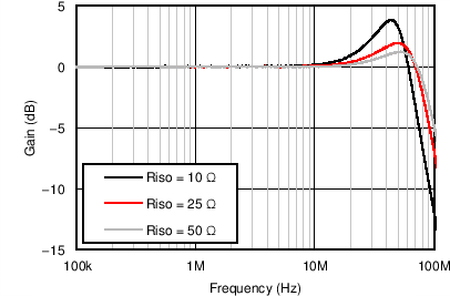
| G = 1, CLOAD = 1.2 nF | ||
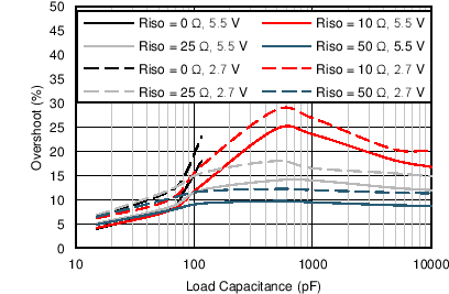
| G = –1, VO = 10 mVPP | ||
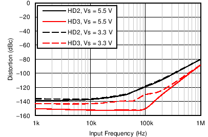
| G = 1, VO = 2 VPP, RLOAD = 600 Ω | ||
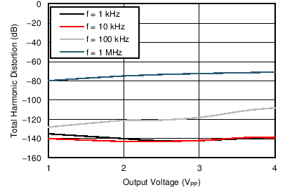
| G = 1, RLOAD = 600 Ω | ||
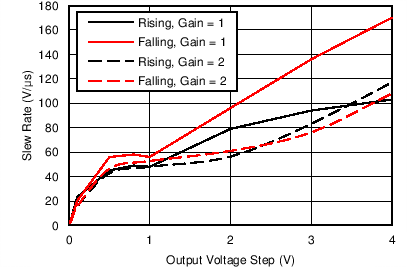
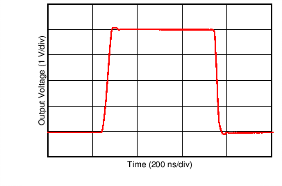
| G = 1, VO = 4-V step | ||
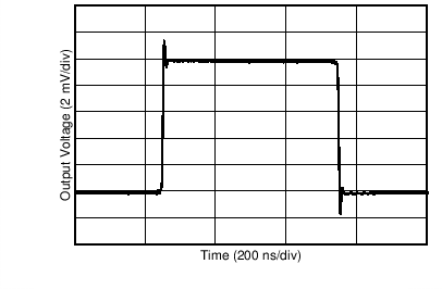
| G = 1, VO = 10-mV step | ||
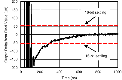
| VO = 3.6-V step at t = 0 s | ||
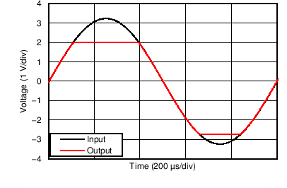
| VS = ±2.75 V, G = 1 | ||
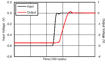
| VS = ±2.75 V, G = 5 | ||
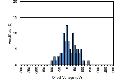
| Distribution taken from 80 amplifiers, TA = 125°C | ||
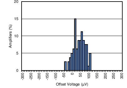
| Distribution taken from 80 amplifiers, TA = –40°C | ||
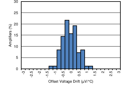
| Distribution taken from 83 amplifiers, TA = –40°C to +125°C |
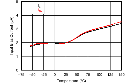
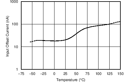
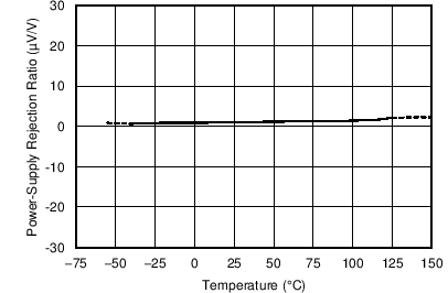
| 2.7 V ≤ VS ≤ 5.5 V | ||
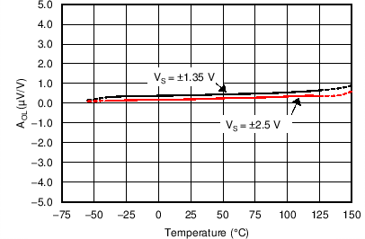
| RLOAD = 600 Ω | ||
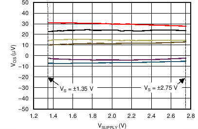
| 6 typical units shown, VS = ±1.35 V to ±2.75 V | ||
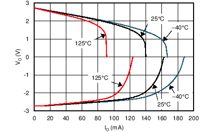
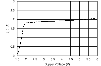
| High-drive mode | ||
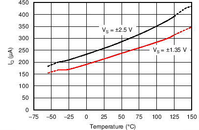
| MODE pin connected to V+ |
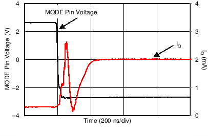
| VS = ±2.75 V | ||
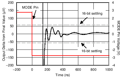
| VO = 3.8 VDC | ||
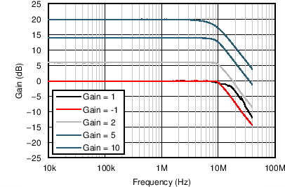
| VO = 2 VPP |
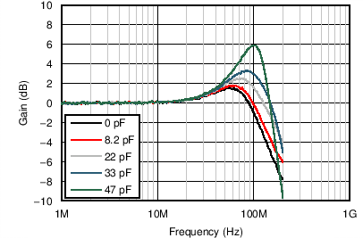
| VO = 10 mVPP , G = 1 |
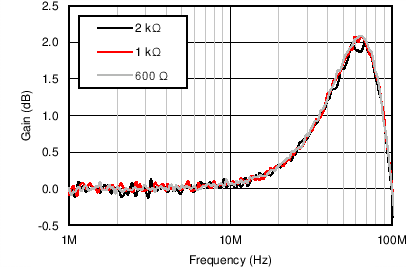
| VO = 10 mVPP , G = 1 |
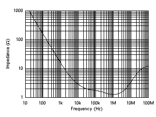
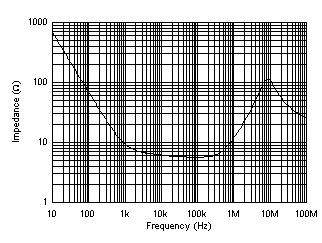
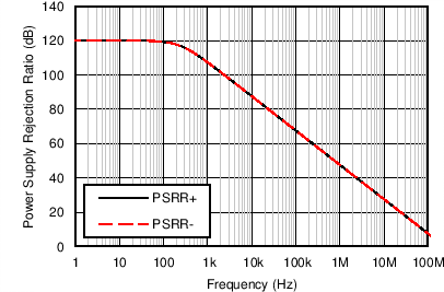
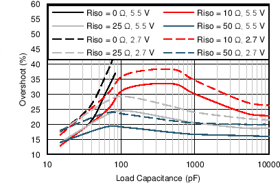
| G = 1, VO = 10 mVPP | ||
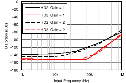
| VS = 5.5 V, VO = 2 VPP, RLOAD = 600 Ω | ||
| G = 2, VO = 2 VPP, RLOAD = 600 Ω | ||
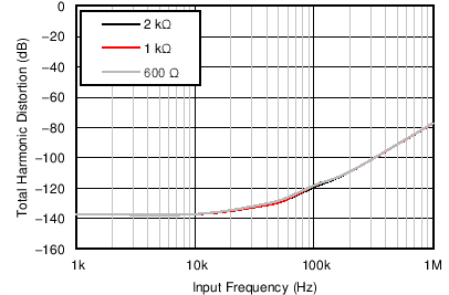
| G = 1, VO = 2 VPP , RLOAD = 600 Ω | ||
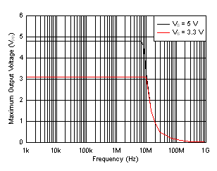
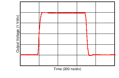
| G = –1, VO = 4-V step | ||
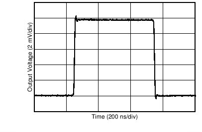
| G = –1, VO = 10-mV step | ||
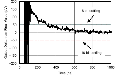
| VO = 3.6-V step at t = 0 s | ||
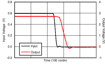
| VS = ±2.75 V, G = 5 | ||
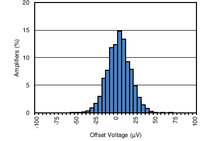
| Distribution taken from 3139 amplifiers | ||
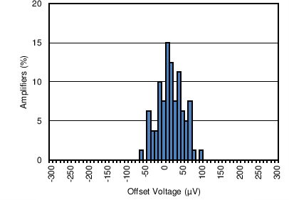
| Distribution taken from 80 amplifiers, TA = 85°C | ||
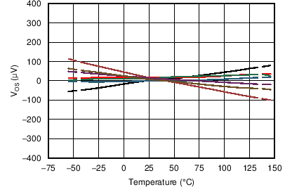
| 7 typical units shown | ||
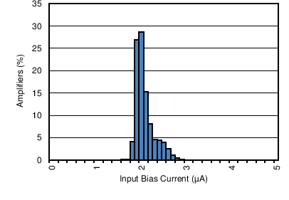
| Distribution taken from 3139 amplifiers |
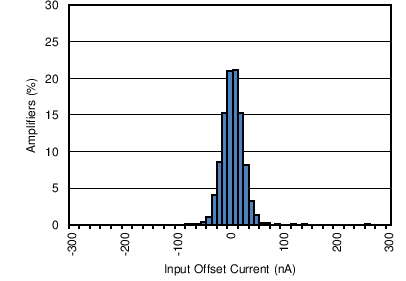
| Distribution taken from 3139 amplifiers |
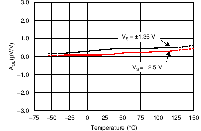
| RLOAD = 10 kΩ | ||
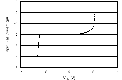
| High-drive mode, VS = ±2.5 V | ||
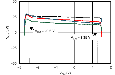
| 6 typical units shown, VS = ±2.5 V | ||
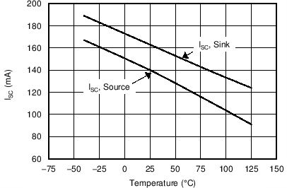
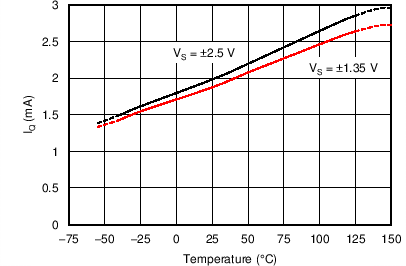
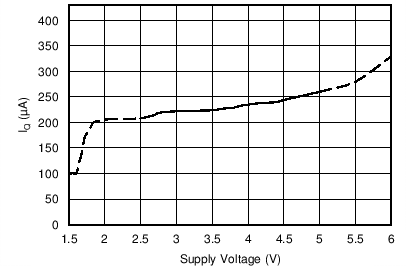
| Low-drive mode, MODE pin connected to V+ |
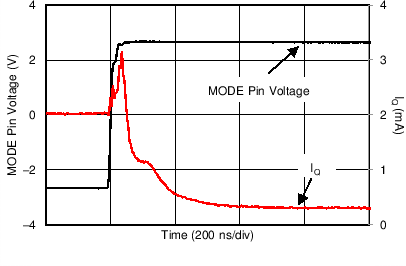
| VS = ±2.75 V | ||
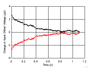
| OPA625 powered on in high-drive mode at t = 0 s, PCB dimensions: 4 in2, 2 layer, FR4 |
