SCPS123F March 2005 – January 2015 PCF8575C
PRODUCTION DATA.
- 1 Features
- 2 Applications
- 3 Description
- 4 Revision History
- 5 Pin Configuration
- 6 Specifications
- 7 Parameter Measurement Information
- 8 Detailed Description
- 9 Application and Implementation
- 10Power Supply Recommendations
- 11Layout
- 12Device and Documentation Support
- 13Mechanical, Packaging, and Orderable Information
Package Options
Mechanical Data (Package|Pins)
Thermal pad, mechanical data (Package|Pins)
- RGE|24
Orderable Information
1 Features
- I2C to Parallel-Port Expander
- Open-Drain Interrupt Output
- Low Standby-Current Consumption of 10 μA Maximum
- Compatible With Most Microcontrollers
- 400-kHz Fast I2C Bus
- Address by Three Hardware Address Pins for Use of up to Eight Devices
- Latched Outputs With High-Current Drive Capability for Directly Driving LEDs
- Latch-Up Performance Exceeds 100 mA Per JESD 78, Class II
- ESD Protection Exceeds JESD 22
- 2000-V Human-Body Model
- 200-V Machine Model
- 1000-V Charged-Device Model
2 Applications
- Telecom Shelters: Filter Units
- Servers
- Routers (Telecom Switching Equipment)
- Personal Computers
- Personal Electronics
- Industrial Automation
- Products with GPIO-Limited Processors
3 Description
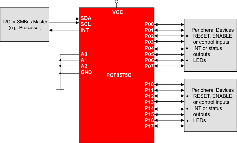
This 16-bit I/O expander for the two-line bidirectional bus (I2C) is designed for 4.5-V to 5.5-V VCC operation.
The PCF8575C provides general-purpose remote I/O expansion for most microcontroller families via the I2C interface serial clock (SCL) and serial data (SDA).
The device features a 16-bit quasi-bidirectional input/output (I/O) port (P07–P00, P17–P10), including latched outputs with high-current drive capability for directly driving LEDs. Each quasi-bidirectional I/O can be used as an input or output without the use of a data-direction control signal. At power on, the I/Os are in 3-state mode. The strong pullup to VCC allows fast-rising edges into heavily loaded outputs. This device turns on when an output is written high and is switched off by the negative edge of SCL. The I/Os should be high before being used as inputs. After power on, as all the I/Os are set to 3-state, all of them can be used as inputs. Any change in setting of the I/Os as either inputs or outputs can be done with the write mode. If a high is applied externally to an I/O that has been written earlier to low, a large current (IOL) flows to GND.
Device Information(1)
| PART NUMBER | PACKAGE (PIN) | BODY SIZE |
|---|---|---|
| PCF8575C | SSOP (24) | 8.20 mm × 5.30 mm |
| QSOP (24) | 8.65 mm × 3.90 | |
| TVSOP (24) | 5.00 mm × 4.50 mm | |
| SOIC (24) | 15.40 mm × 7.50 mm | |
| TSSOP (24) | 7.80 mm × 4.40 mm | |
| QFN (24) | 4.0 mm × 4.0 mm |
- For all available packages, see the orderable addendum at the end of the data sheet.