SLES142B JUNE 2005 – July 2016 PCM1803A
PRODUCTION DATA.
- 1 Features
- 2 Applications
- 3 Description
- 4 Revision History
- 5 Pin Configuration and Functions
- 6 Specifications
- 7 Detailed Description
- 8 Application and Implementation
- 9 Power Supply Recommendations
- 10Layout
- 11Device and Documentation Support
- 12Mechanical, Packaging, and Orderable Information
Package Options
Mechanical Data (Package|Pins)
- DB|20
Thermal pad, mechanical data (Package|Pins)
Orderable Information
8 Application and Implementation
NOTE
Information in the following applications sections is not part of the TI component specification, and TI does not warrant its accuracy or completeness. TI’s customers are responsible for determining suitability of components for their purposes. Customers should validate and test their design implementation to confirm system functionality.
8.1 Application Information
The PCM1803A device is suitable for wide variety of cost-sensitive consumer applications requiring good performance and operation with a 5-V analog supply and 3.3-V digital supply.
8.2 Typical Application
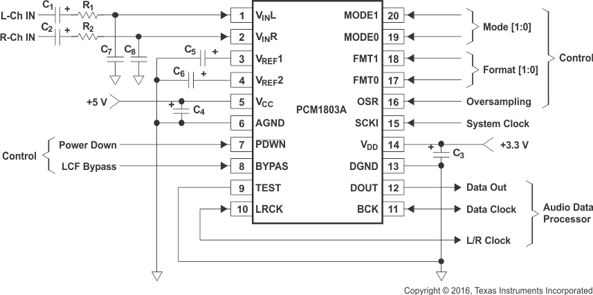
Figure 24 illustrates a typical circuit connection diagram where the cutoff frequency of the input HPF is about 160 kHz.

8.2.1 Design Requirements
For this design example, use the parameters listed in Table 11 as the input parameters.
Table 11. Design Parameters
| DESIGN PARAMETER | EXAMPLE VALUE |
|---|---|
| Analog Input Voltage Range | 0 Vp-p to 3 Vp-p |
| Output | PCM audio data |
| System Clock Input Frequency | 2.048 MHz to 49.152 MHz |
| Output Sampling Frequency | 8 kHz to 96 kHz |
| Power Supply | 3.3 V and 5 V |
8.2.2 Detailed Design Procedure
8.2.2.1 Control Pins
The control pins such as the FMT, MODE, OSR, and BYPASS can be controlled by tying up to VDD, down to GND, or driven with GPIO from the DSP or audio processor.
8.2.2.2 DSP or Audio Processor
In this application a DSP or audio processor is acting as the audio master, and the PCM1803A is acting as the audio slave. This means the DSP or audio processor must be able to output audio clocks that the PCM1803A can use to process audio signals.
8.2.2.3 Input Filters
For the analog input circuit an AC coupling capacitor must be placed in series with the input. This removes the DC component of the input signal. An RC filter can also be implemented to filter out of band noise to reduce aliasing. Equation 1 can be used to calculate the cutoff frequency of the optional RC filter for the input.

8.2.3 Application Curve
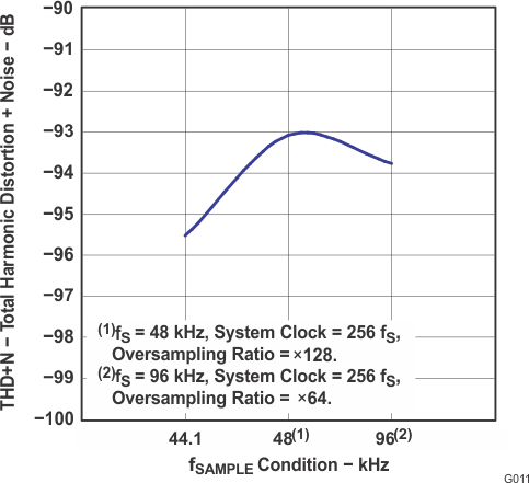
 Figure 25. Total Harmonic Distortion + Noise vs fSAMPLE Condition