SLES230A September 2008 – August 2015 PCM2912A
PRODUCTION DATA.
- 1 Features
- 2 Applications
- 3 Description
- 4 Revision History
- 5 Device Comparison Table
- 6 Pin Configuration and Functions
-
7 Specifications
- 7.1 Absolute Maximum Ratings
- 7.2 ESD Ratings
- 7.3 Recommended Operating Conditions
- 7.4 Thermal Information
- 7.5 Electrical Characteristics
- 7.6
Typical Characteristics
- 7.6.1 ADC Digital Decimation Filter Frequency Response
- 7.6.2 ADC Digital High-Pass Filter Frequency Response
- 7.6.3 ADC Analog Antialiasing Filter Frequency Response
- 7.6.4 DAC Digital Interpolation Filter Frequency Response
- 7.6.5 DAC Analog FIR Filter Frequency Response
- 7.6.6 DAC Analog Low-Pass Filter Frequency Response
- 7.6.7 ADC
- 7.6.8 DAC
- 7.6.9 Supply Current
- 8 Parameter Measurement Information
-
9 Detailed Description
- 9.1 Overview
- 9.2 Functional Block Diagram
- 9.3 Feature Description
- 9.4 Device Functional Modes
- 9.5 Programming
- 10Application and Implementation
- 11Power Supply Recommendations
- 12Layout
- 13Device and Documentation Support
- 14Mechanical, Packaging, and Orderable Information
Package Options
Mechanical Data (Package|Pins)
- PJT|32
Thermal pad, mechanical data (Package|Pins)
Orderable Information
10 Application and Implementation
NOTE
Information in the following applications sections is not part of the TI component specification, and TI does not warrant its accuracy or completeness. TI’s customers are responsible for determining suitability of components for their purposes. Customers should validate and test their design implementation to confirm system functionality.
10.1 Application Information
The VBUS alerts the device when it has been plugged to a USB connection port. The /SSPND flag notifies when the USB input is idle for at least 5 ms; this flag can be used to control or notify subsequent circuits. More functional details can be found in Interface Sequence.
10.2 Typical Application
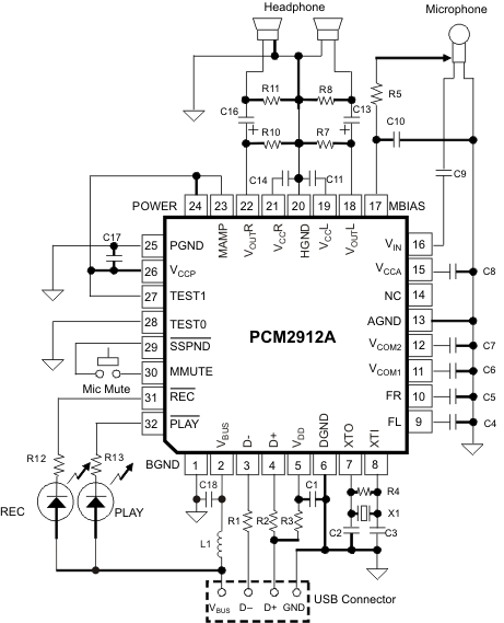
A bus-powered (Hi-power), +20-dB microphone amplifier application example is shown in Figure 37.

NOTE:
X1: 6-MHz crystal resonatorC1, C8, C11, C14, C17, C18: 1 μF ceramic
C2, C3: 10 pF to 33 pF (depending on load capacitance of crystal resonator)
C4, C5: 100 pF ceramic
C6, C10: 3.3 μF
C7: 0.1 μF
C9: 0.22 μF electrolytic (depending on required frequency response for microphone input)
C13, C16: 100 μF electrolytic (depending on required frequency response for headphone output)
R1, R2: 22 Ω to 33 Ω
R3: 1.5 kΩ
R4: 1 MΩ
R5: 1 kΩ (depending on microphone characteristic)
R7, R8, R10, R11: 3.3 kΩ
R12, R13: 820 Ω (depending on LED drive current)
L1: 1 μH (DC resistance < 0.6 Ω)
It is possible to change maximum power if total power of actual application does not require over 100 mA (set POWER = low to configure as low-power device).
NOTE
The circuit in Figure 37 is for information only. Total board design should be considered in order to meet the USB specification as a USB-compliant product.
10.2.1 Design Requirements
For this design example, use the parameters listed in Table 7.
Table 7. Design Parameters
| DESIGN PARAMETER | EXAMPLE VALUE |
|---|---|
| Input voltage range | 4.35 V to 5.25 V |
| Current | 80 mA to 100 mA |
| Input clock frequency | 11.994 MHz to 12.006 MHz |
10.2.2 Detailed Design Procedure
The PCM2912A is a simple design device, as can connect directly to a USB port. The device only requires decoupling capacitors on the voltage source pins and the output filter for the headphone amplifier; a recommended output filter is the one implemented in the PCM2912AEVM, shown in the user's guide (SBAU141).
10.2.3 Application Curves
For the application curves, see the graphs listed in Table 8.
Table 8. Table of Graphs
| FIGURE | ||
|---|---|---|
| ADC Digital Decimation Filter Frequency Response | Overall Characteristic | Figure 1 |
| Stop Band Attenuation | Figure 2 | |
| Passband Ripple | Figure 3 | |
| Transient Band Response | Figure 4 | |
| ADC Digital High-Pass Filter Frequency Response | Stop Band Characteristic | Figure 5 |
| Passband Characteristic | Figure 6 | |
| ADC Analog Antialiasing Filter Frequency Response | Stop Band Characteristic | Figure 7 |
| Passband Characteristic | Figure 8 | |
| DAC Digital Interpolation Filter Frequency Response | Stop Band Attenuation | Figure 9 |
| Passband Ripple | Figure 10 | |
| Transient Band Response | Figure 11 | |
| DAC Analog FIR Filter Frequency Response | Stop Band Characteristic | Figure 12 |
| Passband Characteristic | Figure 13 | |
| DAC Analog Low-Pass Filter Frequency Response | Stop Band Characteristic | Figure 14 |
| Passband Characteristic | Figure 15 | |
| ADC | THD+N at – 1 dB vs Temperature | Figure 16 |
| Dynamic Range and Signal-to-Noise Ratio vs Temperature | Figure 17 | |
| THD+N at – 1 dB vs Supply Voltage | Figure 18 | |
| Dynamic Range and Signal-to-Noise Ratio vs Supply Voltage | Figure 19 | |
| THD+N at – 1 dB vs Sampling Frequency | Figure 20 | |
| Dynamic Range and Signal-to-Noise Ratio vs Sampling Frequency | Figure 21 | |
| DAC | THD+N at 0 dB vs Temperature | Figure 22 |
| Dynamic Range and Signal-to-Noise Ratio vs Temperature | Figure 23 | |
| THD+N at 0 dB vs Supply Voltage | Figure 24 | |
| Dynamic Range and Signal-to-Noise Ratio vs Supply Voltage | Figure 25 | |
| THD+N at 0 dB vs Sampling Frequency | Figure 26 | |
| Dynamic Range and Signal-to-Noise Ratio vs Sampling Frequency | Figure 27 | |
| Supply Current | Supply Current vs Supply Voltage | Figure 28 |
| Supply Current vs Sampling Frequency | Figure 29 | |
| Supply Current vs Temperature at Suspend Mode | Figure 30 |