SNOSBA2B July 2011 – May 2015 SM74101
PRODUCTION DATA.
- 1 Features
- 2 Applications
- 3 Description
- 4 Revision History
- 5 Pin Configuration and Functions
- 6 Specifications
- 7 Detailed Description
- 8 Application and Implementation
- 9 Power Supply Recommendations
- 10Layout
- 11Device and Documentation Support
- 12Mechanical, Packaging, and Orderable Information
Package Options
Mechanical Data (Package|Pins)
- NGG|6
Thermal pad, mechanical data (Package|Pins)
Orderable Information
1 Features
- Renewable Energy Grade
- Compound CMOS and Bipolar Outputs Reduce Output Current Variation
- 7A sink/3A Source Current
- Fast Propagation Times (25 ns Typical)
- Fast Rise and Fall Times (14 ns/12 ns Rise/Fall with 2 nF Load)
- Inverting and Non-Inverting Inputs Provide Either Configuration with a Single Device
- Supply Rail Under-Voltage Lockout Protection
- Dedicated Input Ground (IN_REF) for Split Supply or Single Supply Operation
- Power Enhanced 6-Pin WSON Package (3.0mm x 3.0mm)
- Output Swings from VCC to VEE which can be Negative Relative to Input Ground
2 Applications
- Solar Microinverter
- AC/DC Switch-mode Power Supply
- DC/DC Switch-mode Power Supply
- Solenoid and Motor Drivers
3 Description
The SM74101 MOSFET gate driver provides high peak gate drive current in the tiny WSON-6 package (SOT23 equivalent footprint), with improved power dissipation required for high frequency operation. The compound output driver stage includes MOS and bipolar transistors operating in parallel that together sink more than 7A peak from capacitive loads. Combining the unique characteristics of MOS and bipolar devices reduces drive current variation with voltage and temperature. Under-voltage lockout protection is provided to prevent damage to the MOSFET due to insufficient gate turn-on voltage. The SM74101 provides both inverting and non-inverting inputs to satisfy requirements for inverting and non-inverting gate drive with a single device type.
Device Information(1)
| PART NUMBER | PACKAGE | BODY SIZE (NOM) |
|---|---|---|
| SM74101 | WSON (6) | 3.0 mm x 3.0 mm |
- For all available packages, see the orderable addendum at the end of the data sheet.
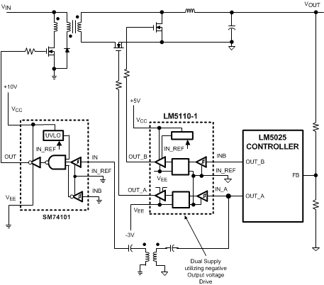
 SM74101 in a DC/DC Forward Topology Power Supply