SNOSBA3D June 2011 – May 2015 SM74104
PRODUCTION DATA.
- 1 Features
- 2 Typical Applications
- 3 Description
- 4 Revision History
- 5 Pin Configuration and Functions
- 6 Detailed Description
- 7 Application and Implementation
- 8 Power Supply Recommendations
- 9 Layout
- 10Device and Documentation Support
Package Options
Mechanical Data (Package|Pins)
Thermal pad, mechanical data (Package|Pins)
Orderable Information
7 Application and Implementation
NOTE
Information in the following applications sections is not part of the TI component specification, and TI does not warrant its accuracy or completeness. TI’s customers are responsible for determining suitability of components for their purposes. Customers should validate and test their design implementation to confirm system functionality.
7.1 Application Information
The SM74104 can drive both a high-side and a low-side MOSFET using only one PWM input control signal. The internal level shifter provides a means for the control input to drive the high-side MOSFET. The SM74104 prevents shoot-through issues through adaptive transition timing and an additional time delay can be added by use of an external resistor at the RT pin.
7.2 Typical Application
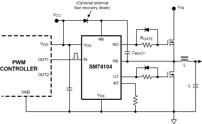
The SM74104 is used to drive MOSFETs connected in a synchronous buck configuration as shown in Figure 20. A single control signal from an external PWM controller provides the control input to drive both the high-side and low-side MOSFET. The HO and LO outputs of the SM74104 can provide very fast switching of the MOSFETs, thereby reducing switching losses and improving the overall efficiency of the system.
 Figure 20. Typical Application
7.2.1 Design Requirements
The RT resistor should be sized such that the appropriate time delay is added between the switching transitions of the top and bottom MOSFETs. The exact RT value will depend on the selected MOSFETs, their switching speeds, and the desired delay time needed to prevent shoot-through. An optional external fast recovery diode should be placed between the VDD and HB pins to minimize the stress on the internal bootstrap diode and decrease the average power dissipation in the IC. An RGATE resistor and a parallel diode may also be placed in the path of the MOSFET gates. The RGATE resistor will decrease the ON switching speed of the MOSFET and can help damp possible oscillations on the line. The parallel diode will provide a current path around RGATE during the OFF switching of the MOSFET, which can ensure fast shut off of the MOSFET to further prevent shoot-through.
7.2.2 Detailed Design Procedure
See Power Supply Recommendations, Layout, and Power Dissipation Considerations for key design considerations regarding the input supply, grounding, component placement, and power calculations specific to the SM74104.
7.2.3 Application Curve
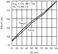
An adaptive circuit in the SM74104 monitors the gate voltages of the top and bottom MOSFETs and triggers a programmable delay generator to prevent both MOSFETs from conducting simultaneously. The timer delay, TRT, can be programmed with a resistor placed between RT and VSS. The value of TRT will vary with the RT resistor value as shown in Figure 21.
 Figure 21. Turn On Delay vs RT Resistor Value