SCLS245M October 1995 – September 2014 SN54AHCT574 , SN74AHCT574
PRODUCTION DATA.
- 1 Features
- 2 Applications
- 3 Description
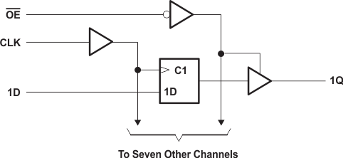
- 4 Simplified Schematic
- 5 Revision History
- 6 Pin Configuration and Functions
- 7 Specifications
- 8 Parameter Measurement Information
- 9 Detailed Description
- 10Application and Implementation
- 11Power Supply Recommendations
- 12Layout
- 13Device and Documentation Support
- 14Mechanical, Packaging, and Orderable Information
Package Options
Refer to the PDF data sheet for device specific package drawings
Mechanical Data (Package|Pins)
- W|20
- J|20
- FK|20
Thermal pad, mechanical data (Package|Pins)
Orderable Information
1 Features
- Inputs are TTL-Voltage Compatible
- Latch-Up Performance Exceeds 250 mA Per JESD 17
-
On Products Compliant to MIL-PRF-38535,
All Parameters are Tested Unless Otherwise Noted. On All Other Products, Production Processing Does Not Necessarily Include Testing of All Parameters. - ESD Protection Exceeds JESD 22
- 2000-V Human-Body Model (A114-A)
- 200-V Machine Model (A115-A)
- 1000-V Charged-Device Model (C101)
2 Applications
- Smartphone Handsets
- PDAs
- Network Switches
- Wearable Health and Fitness Devices
- Televisions (LCDs)
- Power Infrastructures
3 Description
The SNx4AHCT574 devices are octal edge-triggered D-type flip-flops that feature 3-state outputs designed specifically for driving highly capacitive or relatively low-impedance loads.
Device Information(1)
| PART NUMBER | PACKAGE | BODY SIZE (NOM) |
|---|---|---|
| SNx4AHCT574 | SSOP (20) | 7.20 mm × 5.30 mm |
| TVSOP (20) | 5.00 mm × 4.40 mm | |
| SOIC (20) | 12.80 mm × 7.50 mm | |
| PDIP (20) | 25.40 mm × 6.35 mm | |
| TSSOP (20) | 6.50 mm × 4.40 mm |
- For all available packages, see the orderable addendum at the end of the data sheet.
4 Simplified Schematic