SLLSE84D May 2011 – May 2017 SN65HVD101 , SN65HVD102
PRODUCTION DATA.
- 1 Features
- 2 Applications
- 3 Description
- 4 Revision History
- 5 Device Comparison Table
- 6 Pin Configuration and Functions
- 7 Specifications
- 8 Parameter Measurement
-
9 Detailed Description
- 9.1 Overview
- 9.2 Functional Block Diagram
- 9.3
Feature Description
- 9.3.1 Wake-up Detection
- 9.3.2 Current Limit Indication - Short Circuit Current Detection
- 9.3.3 Active Current Limit Condition: VTHL > VCQ ≥ VTHH
- 9.3.4 Inactive Current Limit Condition: VTHL < VCQ < VTHH
- 9.3.5 Over-temperature Detection
- 9.3.6 CQ Current-limit Adjustment
- 9.3.7 Transceiver Function Tables
- 9.3.8 Voltage Regulator (Not Available in SN65HVD102)
- 9.4 Device Functional Modes
- 10Application and Implementation
- 11Power Supply Recommendations
- 12Layout
- 13Device and Documentation Support
- 14Mechanical, Packaging, and Orderable Information
Package Options
Mechanical Data (Package|Pins)
- RGB|20
Thermal pad, mechanical data (Package|Pins)
- RGB|20
Orderable Information
12 Layout
12.1 Layout Guidelines
- Use a 4-layer board with Layer 1 (top layer) for control signals, Layer 2 as Power Ground Layer for L– and GND), Layer 3 for the 24 V supply plane (L+), and Layer 4 for the regulated output supply (VCC_OUT).
- Use entire planes for L+, VCC_OUT, and L– and GND to assure minimum inductance during fast load or transient current changes.
- The L+ terminal must be buffered to ground with a low-ESR ceramic bypass-capacitor. The recommended capacitor value is 1 μF to 4.7 μF. The capacitor must have a voltage rating of 50 V minimum and a X5R or X7R dielectric.
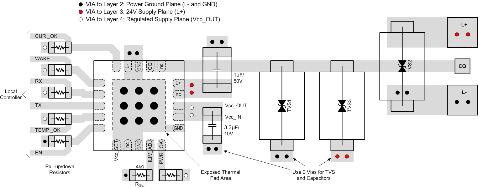
- The optimum placement is closest to the transceiver’s L+ and L– terminals to reduce supply drops during large supply current loads. See Figure 19 for a PCB layout example
- Place TVS diode close to the connector to prevent the transient energy from entering the circuitry.
- Use two vias when connecting TVS diodes or capacitors to the L– and L+ planes to maintain low inductance during fast load or transient current changes.
- Connect all open-drain control outputs and the receiver output via 10 kΩ pull-up resistors to the VCC_OUT plane to provide a defined voltage potential to the system controller inputs when the outputs are high-impedance.
- Connect the transceiver enable pin via a 10 kΩ pull-down resistor to ground, to assure the driver output is disabled during power-up.
- Connect VCC_SET directly to ground to make VCC_OUT = 3.3 V, or leave it open to make VCC_OUT = 5 V.
- Connect VCC_IN directly to VCC_OUT to assure proper voltage regulation.
- Buffer the regulated output voltage at VCC_OUT to ground with a low-ESR, 3.3μF, ceramic bypass-capacitor. The capacitor should have a voltage rating of 10 V minimum and a X5R or X7R dielectric.
12.2 Layout Example
 Figure 19. Layout Example