SLLSFE2 June 2019 SN65HVDA1040B-Q1
PRODUCTION DATA.
- 1 Features
- 2 Applications
- 3 Description
- 4 Revision History
- 5 Pin Configuration and Functions
- 6 Specifications
- 7 Parameter Measurement Information
- 8 Detailed Description
- 9 Application and Implementation
- 10Power Supply Recommendations
- 11Layout
- 12Device and Documentation Support
- 13Mechanical, Packaging, and Orderable Information
Package Options
Mechanical Data (Package|Pins)
- D|8
Thermal pad, mechanical data (Package|Pins)
Orderable Information
3 Description
The SN65HVDA1040B-Q1 device meets or exceeds the specifications of the ISO 11898 standard for use in applications employing a controller area network (CAN). As a CAN transceiver, this device provides differential transmit capability to the bus and differential receive capability to a CAN controller at signaling rates up to 1 megabit per second (Mbps). The signaling rate of a line is the number of voltage transitions that are made per second, expressed in the units bps (bits per second).
The device is designed for operation in especially harsh environments and includes many device protection features such as undervoltage lock out (UVLO), over-temperature thermal shutdown, wide common-mode range, and loss of ground protection. The bus pins are also protected against external cross-wiring, shorts to –27 V to 40 V, and voltage transients according to ISO 7637. The device is qualified for use in automotive applications.
Device Information(1)
| PART NUMBER | PACKAGE | BODY SIZE (NOM) |
|---|---|---|
| SN65HVDA1040B-Q1 | SOIC (8) | 4.90 mm × 3.91 mm |
- For all available packages, see the orderable addendum at the end of the data sheet.
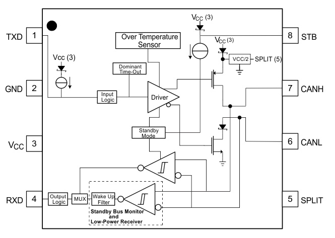
Block Diagram
