SLAS638A January 2009 – October 2015 SN65HVS885
PRODUCTION DATA.
- 1 Features
- 2 Applications
- 3 Description
- 4 Revision History
- 5 Pin Configuration and Functions
- 6 Specifications
- 7 Parameter Measurement Information
- 8 Detailed Description
- 9 Application and Implementation
- 10Power Supply Recommendations
- 11Layout
- 12Device and Documentation Support
- 13Mechanical, Packaging, and Orderable Information
Package Options
Mechanical Data (Package|Pins)
- PWP|28
Thermal pad, mechanical data (Package|Pins)
- PWP|28
Orderable Information
9 Application and Implementation
NOTE
Information in the following applications sections is not part of the TI component specification, and TI does not warrant its accuracy or completeness. TI’s customers are responsible for determining suitability of components for their purposes. Customers should validate and test their design implementation to confirm system functionality.
9.1 Application Information
9.1.1 System-Level EMC
The SN65HVS885 is designed to operate reliably in harsh industrial environments. At a system level, the device is tested according to several international electromagnetic compatibility (EMC) standards.
In addition to the device internal ESD structures, external protection circuitry shown in Figure 13, can be used to absorb as much energy from burst- and surge-transients as possible.
 Figure 13. Typical EMC Protection Circuitry for Supply and Signal Inputs
9.1.2 Input Channel Switching Characteristics
The input stage of the HVS885 is so designed, that for an input resistor RIN = 1.2 kΩ the trip point for signaling an ON-condition is at 9.4 V at 3.6 mA. This trip point satisfies the switching requirements of IEC61131-2 Type 1 and Type 3 switches.
 Figure 14. Switching Characteristics for IEC61131-2 Type 1, 2, and 3 Proximity Switches
For a Type 2 switch application, two inputs are connected in parallel. The current limiters then add to a total maximum current of 7.2 mA. While the return-path (RE-pin), of one input might be used to drive an indicator LED, the RE-pin of the other input channel should be connected to ground (GND).
Paralleling input channels reduces the number of available input channels from an octal Type 1 or Type 3 input to a quad Type 2 input device. Note, that in this configuration output data of an input channel is represented by two shift register bits.
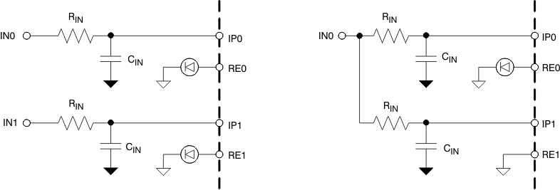 Figure 15. Paralleling Two Type 1 or Type 3 Inputs Into One Type 2 Input
9.1.3 Digital Interface Timing
The digital interface of the SN65HVS885 is SPI compatible and interfaces, isolated or non-isolated, to a wide variety of standard micro controllers.
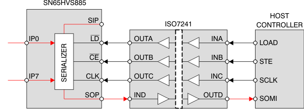 Figure 16. Simple Isolation of the Shift Register Interface
Upon a low-level at the load input, LD, the information of the field inputs, IP0 to IP7 is latched into the shift register. Taking /LD high again blocks the parallel inputs of the shift register from the field inputs. A low-level at the clock-enable input, CE, enables the clock signal, CLK, to serially shift the data to the serial output, SOP. Data is clocked at the rising edge of CLK. Thus after eight consecutive clock cycles all field input data have been clocked out of the shift register and the information of the serial input, SIP, appears at the serial output, SOP.
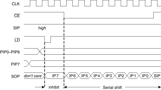 Figure 17. Interface Timing for Parallel-Load and Serial-Shift Operation of the Shift Register
9.1.4 Cascading for High Channel Count Input Modules
Designing high-channel count modules require cascading multiple SN65HVS885 devices. Simply connect the serial output (SOP) of a leading device with the serial input (SIP) of a following device without changing the processor interface.
 Figure 18. Cascading Four SN65HVS885 for a 32-Channel Input Module
9.2 Typical Application
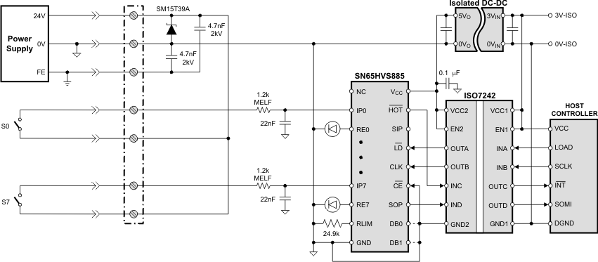 Figure 19. Typical Digital Input Module Application
9.2.1 Design Requirements
The simplified schematic in Figure 19 demonstrates a typical application of the SN65HVS885 for sensing the state of digital switches with 24-V high logic levels. In this application, a 3.3-V host controller must receive the state of 8 switches as a serial input, while remaining isolated from the high voltage power supply.
9.2.2 Detailed Design Procedure
9.2.2.1 Input Stage
Selection of the current limiting resistor RLIM sets the input current limit ILIM for the device. Digital Inputs includes necessary equations for choosing the limiting resistor.
The On/Off voltage thresholds at the device pin VTH(IP+) and VTH(IP-) are fixed to 5.2 V and 4.3 V respectively, however the On/Off voltage thresholds of the field input VTH(IN+) and VTH(IN-) are determined by the value of the series resistor RIN placed between the field input and the device. The threshold voltage VTH(IN+) is determined with the following equation:

Substituting Equation 1 from section 8.3.1, and solving for RIN produces an equation for RIN given a desired on-threshold.

The following equation can be used to calculate the off-threshold voltage given a value for RIN

Figure 20 contains an example input characteristic:
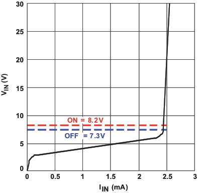 Figure 20. SN65HVS885 Example Input Characteristic
9.2.2.2 Setting Debounce Time
The logic signals at the DB0 and DB1 pins determine the denounce times for the device according to the table in section 6.5. The DB0 and DB1 pins are internally pulled high. Connecting the pins to GND in different configurations allows for selection of 0, 1, or 3ms debounce times. In noisy environments, it is recommended that unused DB pins should be connected externally to a 5 V supply.
9.2.2.3 Using the HOT Indicator
The HOT pin can be used as a visual health indicator for the device. To use the HOT pin as a health indicator, a green LED can be connected (with a series resistor) between the HOT pin and ground. If the device exceeds recommended operating temperature, the LED will turn off. Alternatively, the HOT pin can be connected to the MCU to trigger an interrupt if temperature limits are exceeded.
9.2.2.4 Example: High-Voltage Sensing Application
For the high-voltage sensing application in Figure 19, inputs from each switch (S0-S7) are connected to the 8 parallel inputs (IP0-IP7) of the SN65HVS885 through 1.2kΩ MELF resistors. Small capacitors (22nF) are tied to ground at each input to provide noise protection for the signals. A resistor is added between the RLIM pin and GND to provide a device current limit according to the equation ILIM = 90 V / RLIM. In this example, with a 24.9kΩ resistor, the current limit for the device is set to 3.6mA. LEDs are placed between pins RE0-RE7 to allow for external status observation of the parallel inputs. Finally the SN65HVS885 is connected through a digital isolation device to the host controller to provide galvanic isolation to the external interfaces and to allow for communication between the 5 V SN65HVS885 logic and the 3.3-V host controller. The host controller manages mode switching and clocking of the SN65HVS885 through the digital isolation device.
9.2.3 Application Curve
The application traces acquired in Figure 21 demonstrate typical behavior for the SN65HVD885. The trace names in descending order are: Clock Signal (CE), Clock Enable Input (CE), Load Pulse Input (LD), and Serial Data Output (SOP).
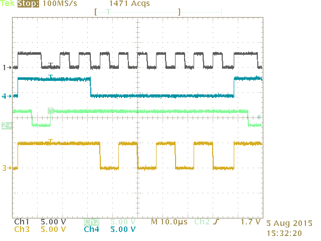 Figure 21. SN65HVD885 Application Measurements