SLLS573D December 2003 – December 2015 SN65MLVD200A , SN65MLVD202A , SN65MLVD204A , SN65MLVD205A
PRODUCTION DATA.
- 1 Features
- 2 Applications
- 3 Description
- 4 Revision History
- 5 Device Comparison Table
- 6 Pin Configuration and Functions
-
7 Specifications
- 7.1 Absolute Maximum Ratings
- 7.2 ESD Ratings
- 7.3 Recommended Operating Conditions
- 7.4 Thermal Information
- 7.5 Electrical Characteristics
- 7.6 Electrical Characteristics - Driver
- 7.7 Electrical Characteristics - Receiver
- 7.8 Electrical Characteristics - BUS Input and Output
- 7.9 Switching Characteristics - Driver
- 7.10 Switching Characteristics - Receiver
- 7.11 Typical Characteristics
- 8 Parameter Measurement Information
- 9 Detailed Description
-
10Application and Implementation
- 10.1 Application Information
- 10.2
Typical Application
- 10.2.1 Design Requirements
- 10.2.2
Detailed Design Procedure
- 10.2.2.1 Supply Voltage
- 10.2.2.2 Supply Bypass Capacitance
- 10.2.2.3 Driver Input Voltage
- 10.2.2.4 Driver Output Voltage
- 10.2.2.5 Termination Resistors
- 10.2.2.6 Receiver Input Signal
- 10.2.2.7 Receiver Input Threshold (Failsafe)
- 10.2.2.8 Receiver Output Signal
- 10.2.2.9 Interconnecting Media
- 10.2.2.10 PCB Transmission Lines
- 10.2.3 Application Curves
- 11Power Supply Recommendations
- 12Layout
- 13Device and Documentation Support
- 14Mechanical, Packaging, and Orderable Information
Package Options
Refer to the PDF data sheet for device specific package drawings
Mechanical Data (Package|Pins)
- D|8
Thermal pad, mechanical data (Package|Pins)
- D|8
Orderable Information
7 Specifications
7.1 Absolute Maximum Ratings
over operating free-air temperature range unless otherwise noted(1)| MIN | MAX | UNIT | |||
|---|---|---|---|---|---|
| Supply voltage(2), VCC | –0.5 | 4 | V | ||
| Input voltage | D, DE, RE | –0.5 | 4 | V | |
| A, B (SN65MLVD200A and SN65MLVD204A) | –1.8 | 4 | V | ||
| A, B (SN65MLVD202A, SN65MLVD205A) | –4 | 6 | V | ||
| Output voltage range | R | –0.3 | 4 | V | |
| Y, Z, A, or B | –1.8 | 4 | V | ||
| Continuous power dissipation | See Thermal Information | ||||
| Storage temperature, Tstg | –65 | 150 | °C | ||
(1) Stresses beyond those listed under Absolute Maximum Ratings may cause permanent damage to the device. These are stress ratings only, and functional operation of the device at these or any other conditions beyond those indicated under Recommended Operating Conditions is not implied. Exposure to absolute-maximum-rated conditions for extended periods may affect device reliability.
(2) All voltage values, except differential I/O bus voltages, are with respect to network ground terminal.
7.2 ESD Ratings
| VALUE | UNIT | ||||
|---|---|---|---|---|---|
| V(ESD) | Electrostatic discharge | Human body model (HBM), per ANSI/ESDA/JEDEC JS-001, all pins(1) | All pins except A, B, Y, and Z | ±4000 | V |
| A, B, Y, and Z | ±8000 | ||||
| Charged device model (CDM), per JEDEC specification JESD22-C101, all pins(2) | All pins | ±1500 | |||
(1) JEDEC document JEP155 states that 500-V HBM allows safe manufacturing with a standard ESD control process.
(2) JEDEC document JEP157 states that 250-V CDM allows safe manufacturing with a standard ESD control process.
7.3 Recommended Operating Conditions
7.4 Thermal Information
| THERMAL METRIC(1) | SN65MLVD200A, SN65MLVD204A |
SN65MLVD202A, SN65MLVD205A |
UNIT | |
|---|---|---|---|---|
| D (SOIC) | D (SOIC) | |||
| 8 PINS | 14 PINS | |||
| RθJA | Junction-to-ambient thermal resistance | 103.9 | 78.9 | °C/W |
| RθJC(top) | Junction-to-case (top) thermal resistance | 50.6 | 39 | °C/W |
| RθJB | Junction-to-board thermal resistance | 44.5 | 33.3 | °C/W |
| ψJT | Junction-to-top characterization parameter | 8.1 | 7.2 | °C/W |
| ψJB | Junction-to-board characterization parameter | 43.9 | 33 | °C/W |
(1) For more information about traditional and new thermal metrics, see the Semiconductor and IC Package Thermal Metrics application report (SPRA953).
7.5 Electrical Characteristics
over recommended operating conditions unless otherwise noted| PARAMETER | TEST CONDITIONS | MIN | TYP(1) | MAX | UNIT | |||
|---|---|---|---|---|---|---|---|---|
| ICC | Supply current | Driver only | RE and DE at VCC, RL = 50 Ω, All others open | 13 | 22 | mA | ||
| Both disabled | RE at VCC, DE at 0 V, RL = No Load, All others open | 1 | 4 | |||||
| Both enabled | RE at 0 V, DE at VCC, RL = 50 Ω, All others open | 16 | 24 | |||||
| Receiver only | RE at 0 V, DE at 0 V, All others open | 4 | 13 | |||||
| PD | Device power dissipation | RL = 50 Ω, Input to D is a 50-MHz 50% duty cycle square wave, DE = high, RE = low, TA = 85°C |
94 | mW | ||||
(1) All typical values are at 25°C and with a 3.3-V supply voltage.
7.6 Electrical Characteristics – Driver
over recommended operating conditions unless otherwise noted| PARAMETER | TEST CONDITIONS | MIN(1) | TYP(2) | MAX | UNIT | |
|---|---|---|---|---|---|---|
| |VAB| or |VYZ| |
Differential output voltage magnitude | See Figure 14 | 480 | 650 | mV | |
| Δ|VAB| or Δ|VYZ| |
Change in differential output voltage magnitude between logic states | –50 | 50 | mV | ||
| VOS(SS) | Steady-state common-mode output voltage | See Figure 15 | 0.8 | 1.2 | V | |
| ΔVOS(SS) | Change in steady-state common-mode output voltage between logic states | –50 | 50 | mV | ||
| VOS(PP) | Peak-to-peak common-mode output voltage | 150 | mV | |||
| VY(OC) or VA(OC) |
Maximum steady-state open-circuit output voltage | See Figure 19 | 0 | 2.4 | V | |
| VZ(OC) or VB(OC) |
Maximum steady-state open-circuit output voltage | 0 | 2.4 | V | ||
| VP(H) | Voltage overshoot, low-to-high level output | See Figure 17 | 1.2 VSS | V | ||
| VP(L) | Voltage overshoot, high-to-low level output | –0.2 VSS | V | |||
| IIH | High-level input current (D, DE) | VIH = 2 V to VCC | 0 | 10 | µA | |
| IIL | Low-level input current (D, DE) | VIL = GND to 0.8 V | 0 | 10 | µA | |
| |IOS| | Differential short-circuit output current magnitude | See Figure 4 | 24 | mA | ||
| IOZ | High-impedance state output current (driver only) | –1.4 V ≤ (VY or VZ) ≤ 3.8 V, Other output = 1.2 V |
–15 | 10 | µA | |
| IO(OFF) | Power-off output current | –1.4 V ≤ (VY or VZ) ≤ 3.8 V, Other output = 1.2 V, 0 V ≤ VCC≤ 1.5 V | –10 | 10 | µA | |
| CY or CZ | Output capacitance | VI = 0.4 sin(30E6πt) + 0.5 V,(3)
Other input at 1.2 V, driver disabled |
3 | pF | ||
| CYZ | Differential output capacitance | VAB = 0.4 sin(30E6πt) V, (3)
Driver disabled |
2.5 | pF | ||
| CY/Z | Output capacitance balance, (CY/CZ) | 0.99 | 1.01 | |||
(1) The algebraic convention in which the least positive (most negative) limit is designated as minimum is used in this data sheet.
(2) All typical values are at 25°C and with a 3.3-V supply voltage.
(3) HP4194A impedance analyzer (or equivalent)
7.7 Electrical Characteristics – Receiver
over recommended operating conditions unless otherwise noted| PARAMETER | TEST CONDITIONS | MIN | TYP(1) | MAX | UNIT | ||
|---|---|---|---|---|---|---|---|
| VIT+ | Positive-going differential input voltage threshold | Type 1 | See Figure 9, Table 1, and Table 2 | 50 | mV | ||
| Type 2 | 150 | ||||||
| VIT- | Negative-going differential input voltage threshold | Type 1 | –50 | mV | |||
| Type 2 | 50 | ||||||
| VHYS | Differential input voltage hysteresis, (VIT+ – VIT–) | Type 1 | 25 | mV | |||
| Type 2 | 0 | ||||||
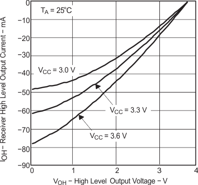
| VOH | High-level output voltage (R) | IOH = –8 mA | 2.4 | V | |||
| VOL | Low-level output voltage (R) | IOL = 8 mA | 0.4 | V | |||
| IIH | High-level input current (RE) | VIH = 2 V to VCC | –10 | 0 | µA | ||
| IIL | Low-level input current (RE) | VIL = GND to 0.8 V | –10 | 0 | µA | ||
| IOZ | High-impedance output current (R) | VO = 0 V or 3.6 V | –10 | 15 | µA | ||
| CA or CB | Input capacitance | VI = 0.4 sin(30E6πt) + 0.5 V(2), Other input at 1.2 V |
3 | pF | |||
| CAB | Differential input capacitance | VAB = 0.4 sin(30E6πt) V(2) | 2.5 | pF | |||
| CA/B | Input capacitance balance, (CA/CB) | 0.99 | 1.01 | ||||
(1) All typical values are at 25°C and with a 3.3-V supply voltage.
(2) HP4194A impedance analyzer (or equivalent)
7.8 Electrical Characteristics – BUS Input and Output
over recommended operating conditions unless otherwise noted| PARAMETER | TEST CONDITIONS | MIN | TYP(1) | MAX | UNIT | |||
|---|---|---|---|---|---|---|---|---|
| IA | Receiver or transceiver with driver disabled input current | VA = 3.8 V, | VB = 1.2 V, | 0 | 32 | µA | ||
| VA = 0 V or 2.4 V, | VB = 1.2 V | –20 | 20 | |||||
| VA = –1.4 V, | VB = 1.2 V | –32 | 0 | |||||
| IB | Receiver or transceiver with driver disabled input current | VB = 3.8 V, | VA = 1.2 V | 0 | 32 | µA | ||
| VB = 0 V or 2.4 V, | VA = 1.2 V | –20 | 20 | |||||
| VB = –1.4 V, | VA = 1.2 V | –32 | 0 | |||||
| IAB | Receiver or transceiver with driver disabled differential input current (IA – IB) | VA = VB, | 1.4 ≤ VA ≤ 3.8 V | –4 | 4 | µA | ||
| IA(OFF) | Receiver or transceiver power-off input current | VA = 3.8 V, | VB = 1.2 V, | 0 V ≤ VCC ≤ 1.5 V | 0 | 32 | µA | |
| VA = 0 V or 2.4 V, | VB = 1.2 V, | 0 V ≤ VCC ≤ 1.5 V | –20 | 20 | ||||
| VA = –1.4 V, | VB = 1.2 V, | 0 V ≤ VCC ≤ 1.5 V | –32 | 0 | ||||
| IB(OFF) | Receiver or transceiver power-off input current | VB = 3.8 V, | VA = 1.2 V, | 0 V ≤ VCC ≤ 1.5 V | 0 | 32 | µA | |
| VB = 0 V or 2.4 V, | VA = 1.2 V, | 0 V ≤ VCC ≤ 1.5 V | –20 | 20 | ||||
| VB = –1.4 V, | VA = 1.2 V, | 0 V ≤ VCC ≤ 1.5 V | –32 | 0 | ||||
| IAB(OFF) | Receiver input or transceiver power-off differential input current (IA – IB) | VA = VB, 0 V ≤ VCC ≤ 1.5 V, –1.4 ≤ VA ≤ 3.8 V | –4 | 4 | µA | |||
| CA | Transceiver with driver disabled input capacitance | VA = 0.4 sin (30E6πt) + 0.5 V(2), VB = 1.2 V | 5 | pF | ||||
| CB | Transceiver with driver disabled input capacitance | VB = 0.4 sin (30E6πt) + 0.5 V(2), VA = 1.2 V | 5 | pF | ||||
| CAB | Transceiver with driver disabled differential input capacitance | VAB = 0.4 sin (30E6πt)V(2) | 3 | pF | ||||
| CA/B | Transceiver with driver disabled input capacitance balance, (CA/CB) | 0.99 | 1.01 | |||||
(1) All typical values are at 25°C and with a 3.3-V supply voltage.
(2) HP4194A impedance analyzer (or equivalent)
7.9 Switching Characteristics – Driver
over recommended operating conditions unless otherwise noted| PARAMETER | TEST CONDITIONS | MIN | TYP(1) | MAX | UNIT | |
|---|---|---|---|---|---|---|
| tpLH | Propagation delay time, low-to-high-level output | See Figure 17 | 2 | 2.5 | 3.5 | ns |
| tpHL | Propagation delay time, high-to-low-level output | 2 | 2.5 | 3.5 | ns | |
| tr | Differential output signal rise time | 2 | 2.6 | 3.2 | ns | |
| tf | Differential output signal fall time | 2 | 2.6 | 3.2 | ns | |
| tsk(p) | Pulse skew (|tpHL – tpLH|) | 30 | 150 | ps | ||
| tsk(pp) | Part-to-part skew (2) | 0.9 | ns | |||
| tjit(per) | Period jitter, rms (1 standard deviation)(3) | 50-MHz clock input(4) | 2 | 3 | ps | |
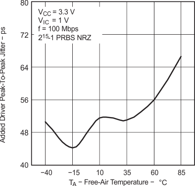
| tjit(pp) | Peak-to-peak jitter(3)(6) | 100 Mbps 215 –1 PRBS input(5) | 55 | 150 | ps | |
| tPHZ | Disable time, high-level-to-high-impedance output | See Figure 18 | 4 | 7 | ns | |
| tPLZ | Disable time, low-level-to-high-impedance output | 4 | 7 | ns | ||
| tPZH | Enable time, high-impedance-to-high-level output | 4 | 7 | ns | ||
| tPZL | Enable time, high-impedance-to-low-level output | 4 | 7 | ns | ||
(1) All typical values are at 25°C and with a 3.3-V supply voltage.
(2) Part-to-part skew is defined as the difference in propagation delays between two devices that operate at the same V/T conditions.
(3) Jitter is ensured by design and characterization. Stimulus jitter has been subtracted from the numbers.
(4) tr = tf = 0.5 ns (10% to 90%), measured over 30K samples.
(5) tr = tf = 0.5 ns (10% to 90%), measured over 100K samples.
(6) Peak-to-peak jitter includes jitter due to pulse skew (tsk(p)).
7.10 Switching Characteristics – Receiver
over recommended operating conditions unless otherwise noted| PARAMETER | TEST CONDITIONS | MIN | TYP(1) | MAX | UNIT | ||
|---|---|---|---|---|---|---|---|
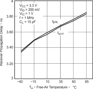
| tPLH | Propagation delay time, low-to-high-level output | CL = 15 pF, See Figure 22 | 2 | 3.6 | 6 | ns | |
| tPHL | Propagation delay time, high-to-low-level output | 2 | 3.6 | 6 | ns | ||
| tr | Output signal rise time | 1 | 2.3 | ns | |||
| tf | Output signal fall time | 1 | 2.3 | ns | |||
| tsk(p) | Pulse skew (|tpHL – tpLH|) | Type 1 | 100 | 300 | ps | ||
| Type 2 | 300 | 500 | ps | ||||
| tsk(pp) | Part-to-part skew(2) | 1 | ns | ||||
| tjit(per) | Period jitter, rms (1 standard deviation)(3) | 50-MHz clock input(4) | 4 | 7 | ps | ||
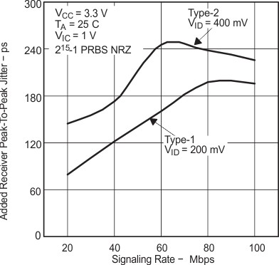
| tjit(pp) | Peak-to-peak jitter(3) (6) | Type 1 | 100 Mbps 215 –1 PRBS input(5) | 200 | 700 | ps | |
| Type 2 | 225 | 800 | ps | ||||
| tPHZ | Disable time, high-level-to-high-impedance output | See Figure 23 | 6 | 10 | ns | ||
| tPLZ | Disable time, low-level-to-high-impedance output | 6 | 10 | ns | |||
| tPZH | Enable time, high-impedance-to-high-level output | 10 | 15 | ns | |||
| tPZL | Enable time, high-impedance-to-low-level output | 10 | 15 | ns | |||
(1) All typical values are at 25°C and with a 3.3-V supply voltage.
(2) Part-to-part skew is defined as the difference in propagation delays between two devices that operate at the same V/T conditions.
(3) Jitter is ensured by design and characterization. Stimulus jitter has been subtracted from the numbers.
(4) VID = 200 mVpp (MLVD200A, 202A), VID = 400 mVpp (MLVD204A, 205A), Vcm = 1 V, tr = tf = 0.5 ns (10% to 90%), measured over 30K samples.
(5) VID = 200 mVpp (MLVD200A, 202A), VID = 400 mVpp (MLVD204A, 205A), Vcm = 1 V, tr = tf = 0.5 ns (10% to 90%), measured over 100K samples.
(6) Peak-to-peak jitter includes jitter due to pulse skew (tsk(p))
7.11 Typical Characteristics


vs Low-Level Output Voltage


vs Clock Frequency

vs Free-Air Temperature

vs Signaling Rate


vs High-Level Output Voltage

vs Free-Air Temperature


vs Clock Frequency

vs Free-Air Temperature