SCLS226K October 1995 – July 2014 SN54AHC244 , SN74AHC244
PRODUCTION DATA.
- 1 Features
- 2 Applications
- 3 Description
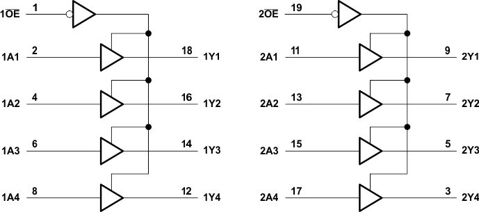
- 4 Simplified Schematic
- 5 Revision History
- 6 Pin Configuration and Functions
- 7 Specifications
- 8 Parameter Measurement Information
- 9 Detailed Description
- 10Application and Implementation
- 11Power Supply Recommendations
- 12Layout
- 13Device and Documentation Support
- 14Mechanical, Packaging, and Orderable Information
Package Options
Refer to the PDF data sheet for device specific package drawings
Mechanical Data (Package|Pins)
- DGV|20
- DB|20
- NS|20
- N|20
- DW|20
- PW|20
Thermal pad, mechanical data (Package|Pins)
- PW|20
Orderable Information
2 Applications
- Network Switches
- Power Infrastructures
- PCs and Notebooks
- Wearable Health and Fitness Devices
- Tests and Measurements
3 Description
These octal buffers and drivers are designed specifically to improve the performance and density of 3-state memory-address drivers, clock drivers, and bus-oriented receivers and transmitters.
Device Information(1)
| PART NUMBER | PACKAGE | BODY SIZE (NOM) |
|---|---|---|
| SNx4AHC244 | SSOP (20) | 7.20 mm × 5.30 mm |
| SOIC (20) | 12.80 mm × 7.50 mm | |
| PDIP (20) | 24.33 mm × 6.35 mm | |
| TSSOP (20) | 12.60 mm × 5.30 mm | |
| VQFN (20) | 4.50 mm × 3.50 mm |
- For all available packages, see the orderable addendum at the end of the data sheet.
4 Simplified Schematic