SDLS146B October 1976 – September 2016 SN54LS245 , SN74LS245
- 1 Features
- 2 Applications
- 3 Description
- 4 Revision History
- 5 Device Comparison Table
- 6 Pin Configuration and Functions
- 7 Specifications
- 8 Parameter Measurement Information
- 9 Detailed Description
- 10Application and Implementation
- 11Power Supply Recommendations
- 12Layout
- 13Device and Documentation Support
- 14Mechanical, Packaging, and Orderable Information
Package Options
Refer to the PDF data sheet for device specific package drawings
Mechanical Data (Package|Pins)
- DB|20
- NS|20
- N|20
- DW|20
Thermal pad, mechanical data (Package|Pins)
Orderable Information
6 Pin Configuration and Functions
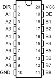
J, W, DB, DW, N, or NS Package
20-Pin CDIP, CFP, SSOP, SOIC, PDIP, or SO
Top View

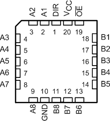
FK Package
20-Pin LCCC
Top View

Pin Functions
| PIN | I/O | DESCRIPTION | |
|---|---|---|---|
| NO. | NAME | ||
| 1 | DIR | I | Controls signal direction; Low = Bx to Ax, High = Ax to Bx |
| 2 | A1 | I/O | Channel 1, A side |
| 3 | A2 | I/O | Channel 2, A side |
| 4 | A3 | I/O | Channel 3, A side |
| 5 | A4 | I/O | Channel 4, A side |
| 6 | A5 | I/O | Channel 5, A side |
| 7 | A6 | I/O | Channel 6, A side |
| 8 | A7 | I/O | Channel 7, A side |
| 9 | A8 | I/O | Channel 8, A side |
| 10 | GND | — | Ground |
| 11 | B8 | O/I | Channel 8, B side |
| 12 | B7 | O/I | Channel 7, B side |
| 13 | B6 | O/I | Channel 6, B side |
| 14 | B5 | O/I | Channel 5, B side |
| 15 | B4 | O/I | Channel 4, B side |
| 16 | B3 | O/I | Channel 3, B side |
| 17 | B2 | O/I | Channel 2, B side |
| 18 | B1 | O/I | Channel 1, B side |
| 19 | OE | I | Active low output enable; Low = all channels active, High = all channels disabled (high impedance) |
| 20 | VCC | — | Power supply |