SCES885 April 2017 SN74LVC1G80-Q1
PRODUCTION DATA.
- 1 Features
- 2 Applications
- 3 Description
- 4 Revision History
- 5 Pin Configuration and Functions
-
6 Specifications
- 6.1 Absolute Maximum Ratings
- 6.2 ESD Ratings
- 6.3 Recommended Operating Conditions
- 6.4 Thermal Information
- 6.5 Electrical Characteristics
- 6.6 Timing Requirements: TA = -40°C to +85°C
- 6.7 Timing Requirements: TA = -40°C to +125°C
- 6.8 Switching Characteristics: TA = -40°C to +85°C, CL = 15 pF
- 6.9 Switching Characteristics: TA = -40°C to +85°C, CL = 30 pF or 50 pF
- 6.10 Switching Characteristics: TA = -40°C to +125°C, CL = 30 pF or 50 pF
- 6.11 Operating Characteristics
- 6.12 Typical Characteristics
- 7 Parameter Measurement Information
- 8 Detailed Description
- 9 Application and Implementation
- 10Power Supply Recommendations
- 11Layout
- 12Device and Documentation Support
- 13Mechanical, Packaging, and Orderable Information
Package Options
Mechanical Data (Package|Pins)
- DCK|5
Thermal pad, mechanical data (Package|Pins)
Orderable Information
1 Features
- Qualified for Automotive Applications
- AEC-Q100 Qualified With the Following Results:
- ±4000-V Human-Body Model (HBM) ESD Classification Level 3A
- ±1000-V Charged-Device Model (CDM) ESD Classification Level C5
- Supports 5-V VCC Operation
- Inputs Accept Voltages to 5.5 V
- Supports Down Translation to VCC
- Maximum tpd of 6 ns at 3.3 V
- Low Power Consumption, 10-µA Max ICC
- ±24-mA Output Drive at 3.3 V
- Ioff supports Partial-Power-Down Mode and Back-Drive Protection
2 Applications
- Automotive Infotainment
- Automotive Cluster
- Automotive ADAS
- Automotive Body Electronics
- Automotive HEV/EV Powertrain
3 Description
The SN74LVC1G80-Q1 device is an automotive AEC-Q100 qualified, single positive-edge-triggered D-type flip-flop that is designed for 1.65-V to 5.5-V VCC operation.
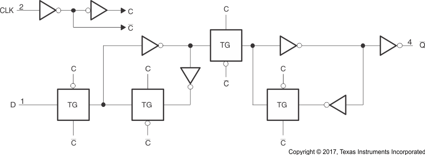
When data at the data (D) input meets the setup time requirement, the data is transferred to the Q output on the positive-going edge of the clock pulse. Clock triggering occurs at a voltage level and is not directly related to the rise time of the clock pulse. Following the hold-time interval, data at the D input can be changed without affecting the level at the output.
This device is fully specified for partial-power-down applications using Ioff. The Ioff circuitry disables the outputs when the device is powered down. This inhibits current backflow into the device which prevents damage to the device.
Device Information(1)
| PART NUMBER | PACKAGE | BODY SIZE |
|---|---|---|
| SN74LVC1G80-Q1 | SC70 (5) | 2.00 mm × 1.25 mm |
- For all available packages, see the orderable addendum at the end of the data sheet.
Logic Diagram (Positive Logic)
