SCES221S April 1999 – November 2016 SN74LVC1G80
PRODUCTION DATA.
- 1 Features
- 2 Applications
- 3 Description
- 4 Revision History
- 5 Pin Configuration and Functions
-
6 Specifications
- 6.1 Absolute Maximum Ratings
- 6.2 ESD Ratings
- 6.3 Recommended Operating Conditions
- 6.4 Thermal Information
- 6.5 Electrical Characteristics
- 6.6 Timing Requirements: TA = -40°C to +85°C
- 6.7 Timing Requirements: TA = -40°C to +125°C
- 6.8 Switching Characteristics: TA = -40°C to +85°C, CL = 15 pF
- 6.9 Switching Characteristics: TA = -40°C to +85°C, CL = 30 pF or 50 pF
- 6.10 Switching Characteristics: TA = -40°C to +125°C, CL = 30 pF or 50 pF
- 6.11 Operating Characteristics
- 6.12 Typical Characteristics
- 7 Parameter Measurement Information
- 8 Detailed Description
- 9 Application and Implementation
- 10Power Supply Recommendations
- 11Layout
- 12Device and Documentation Support
- 13Mechanical, Packaging, and Orderable Information
Package Options
Refer to the PDF data sheet for device specific package drawings
Mechanical Data (Package|Pins)
- DBV|5
- DCK|5
- YZP|5
Thermal pad, mechanical data (Package|Pins)
Orderable Information
8 Detailed Description
8.1 Overview
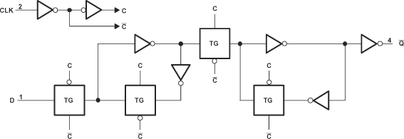
The SN74LVC1G80 is a single positive-edge-trigger D-type flip-flop. Data at the input (D) is transferred to the output (Q) on the positive-going edge of the clock pulse when the setup time requirement is met. Because the clock triggering occurs at a voltage level, it is not directly related to the rise time of the clock pulse. This allows for data at the input to be changed without affecting the level at the output, following the hold-time interval.
8.2 Functional Block Diagram
 Figure 4. Logic Diagram (Positive Logic)
8.3 Feature Description
This device has a wide operating VCC range of 1.65 V to 5.5 V. The wide operating range allows for a broad range of systems the device can be used in. The output can handle This device is full specified for partial-power-down applications. When VCC = 0, the Ioff circuitry disables the outputs, preventing damaging current backflow through the device.
8.4 Device Functional Modes
Table 1 lists the functional modes of the SN74LVC1G80.
Table 1. Function Table
| INPUTS | OUTPUT Q |
|
|---|---|---|
| CLK | D | |
| ↑ | H | L |
| ↑ | L | H |
| L | X | Q0 |