SCES366L August 2001 – October 2015 SN74LVC3G34
PRODUCTION DATA.
- 1 Features
- 2 Applications
- 3 Description
- 4 Revision History
- 5 Pin Configuration and Functions
- 6 Specifications
- 7 Parameter Measurement Information
- 8 Detailed Description
- 9 Application and Implementation
- 10Power Supply Recommendations
- 11Layout
- 12Device and Documentation Support
- 13Mechanical, Packaging, and Orderable Information
Package Options
Refer to the PDF data sheet for device specific package drawings
Mechanical Data (Package|Pins)
- DCU|8
- YZP|8
- DCT|8
Thermal pad, mechanical data (Package|Pins)
Orderable Information
1 Features
-
Available in the Texas Instruments
NanoFree™ Package - Supports 5.5-V VCC Operation
- Inputs Accept Voltages to 5.5 V
- Max tpd of 4.1 ns at 3.3 V
- Low Power Consumption, 10-µA Maximum ICC
- ±24-mA Output Drive at 3.3 V
- Typical VOLP (Output Ground Bounce)
<0.8 V at VCC = 3.3 V, TA = 25°C - Typical VOHV (Output VOH Undershoot)
>2 V at VCC = 3.3 V, TA = 25°C - Ioff Supports Live Insertion, Partial-Power-Down Mode, and Back-Drive Protection
- Can Be Used as a Down Translator to Translate Inputs From a Maximum of 5.5 V Down to the VCC Level
- Latch-Up Performance Exceeds 100 mA Per
JESD 78, Class II - ESD Protection Exceeds JESD 22
- 2000-V Human Body Model (A114-A)
- 200-V Machine Model (A115-A)
- 1000-V Charged-Device Model (C101)
2 Applications
- AV Receivers
- Audio Docks: Portable
- Blu-ray Players and Home Theaters
- DVD Recorders and Players
- Embedded PCs
- MP3 Players and Recorders (Portable Audio)
- Personal Digital Assistant (PDA)
- Power: Telecom/Server AC/DC Supply: Single Controller: Analog and Digital
- Solid-State Drive (SSD): Client and Enterprise
- TV: LCD/Digital and High-Definition (HDTV)
- Tablets: Enterprise
- Video Analytics: Servers
- Wireless Headsets, Keyboards, and Mice
3 Description
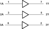
The SN74LVC3G34 device is a triple buffer gate designed for 1.65-V to 5.5-V VCC operation. The SN74LVC3G34 device performs the Boolean function Y = A in positive logic.
NanoFree package technology is a major breakthrough in IC packaging concepts, using the die as the package.
This device is fully specified for partial-power-down applications using Ioff. The Ioff circuitry disables the outputs, preventing damaging current backflow through the device when it is powered down.
Device Information(1)
| PART NUMBER | PACKAGE | BODY SIZE (NOM) |
|---|---|---|
| SN74LVC3G34DCT | SM8 (8) | 2.95 mm × 2.80 mm |
| SN74LVC3G34DCU | VSSOP (8) | 2.30 mm × 2.00 mm |
| SN74LVC3G34YZP | DSBGA (8) | 1.91 mm × 0.91 mm |
- For all available packages, see the orderable addendum at the end of the data sheet.
Simplified Schematic

4 Revision History
Changes from J Revision (Feburary 2007) to K Revision
- Updated document to new TI data sheet format.Go
- Removed Ordering Information table.Go
- Updated Features sectionGo
- Updated operating temperature range.Go
Changes from K Revision (November 2013) to L Revision
- Added Applications, Device Information table, Pin Configuration and Functions section, ESD Ratings table, Thermal Information table, Typical Characteristics section, Feature Description section, Device Functional Modes, Application and Implementation section, Power Supply Recommendations section, Layout section, Device and Documentation Support section, and Mechanical, Packaging, and Orderable Information section Go
- Deleted part number from Switching Characteristics table headers.Go