SCAS585Q November 1996 – December 2022 SN74LVCC3245A
PRODMIX
- 1 Features
- 2 Applications
- 3 Description
- 4 Revision History
- 5 Pin Configuration and Functions
- 6 Specifications
- 7 Parameter Measurement Information
- 8 Detailed Description
- 9 Power Supply Recommendations
- 10Layout
- 11Device and Documentation Support
- 12Mechanical, Packaging, and Orderable Information
Package Options
Mechanical Data (Package|Pins)
Thermal pad, mechanical data (Package|Pins)
- DW|24
Orderable Information
3 Description
The SN74LVCC3245A device is 8-bit (octal) noninverting bus transceiver contains two separate supply rails. The B port is designed to track VCCB, which accepts voltages from 3 V to 5.5 V, and the A port is designed to track VCCA, which operates at 2.3 V to 3.6 V. This allows for translation from a 3.3-V to a 5-V system environment and vice versa, from a
2.5-V to a 3.3-V system environment and vice versa.
Package Information(1)
| PART NUMBER | PACKAGE | BODY SIZE (NOM) |
|---|---|---|
| SN74LVCC3245A | DB (SSOP, 24) | 8.65 mm × 3.90 mm |
| DW (SOIC, 24) | 15.40 mm × 7.50 mm | |
| DBQ (SSOP, 24) | 8.20 mm × 5.30 mm | |
| NS (SO, 24) | 15.00 mm × 5.30 mm | |
| PW (TSSOP, 24) | 7.80 mm × 4.40 mm |
(1) For all available packages, see the orderable addendum at the end of the data sheet.
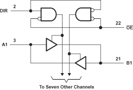
 Functional Block Diagram