SLLSE81A March 2011 – March 2016 SN75LVCP600S
PRODUCTION DATA.
- 1 Features
- 2 Applications
- 3 Description
- 4 Revision History
- 5 Pin Configuration and Functions
- 6 Specifications
- 7 Parameter Measurement Information
- 8 Detailed Description
- 9 Application and Implementation
- 10Power Supply Recommendations
- 11Layout
- 12Device and Documentation Support
- 13Mechanical, Packaging, and Orderable Information
Package Options
Mechanical Data (Package|Pins)
- DSK|10
Thermal pad, mechanical data (Package|Pins)
- DSK|10
Orderable Information
1 Features
- Single 3.3-V Supply
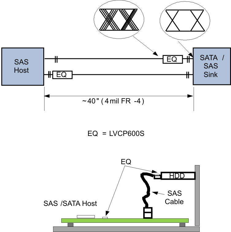
- Suitable to Receive 6-Gbps Data Over up to >40 Inches (1 m) of FR4 PCB
- Two-Level RX and TX Equalization
- RX→ 7, 15 dB
- TX→ 0, –1.3 dB
- Pin-Selectable SATA/SAS Signaling
- Programmable Squelch Threshold for Long Channels
- Low Power in Active, Partial, and Slumber States
- 106 mW Typical (Active Mode at 6 Gbps)
- <11 mW (When Link in Partial and Slumber State)
- Ultra-small Package for Optimal Placement
- 10-Pad 2.5-mm × 2.5-mm QFN
- High ESD-Transient Protection
- HBM: 9,000 V
- CDM: 1,500 V
- MM: 200 V
2 Applications
- Notebook and Desktop PCs
- Docking Stations
- Active Cable
- Servers
- Workstations
3 Description
The SN75LVCP600S is a single-channel SATA/SAS signal conditioner supporting data rates up to 6 Gbps. The device complies with SATA physical spec rev 3.0 and SAS electrical spec 2.0. The SN75LVCP600S operates from a single 3.3-V supply and has 100-Ω line termination with a self-biasing feature, making the device suitable for AC coupling. The inputs incorporate an out-of-band (OOB) detector, which automatically squelches the output while maintaining a stable common-mode voltage compliant to the SATA/SAS link.
The SN75LVCP600S handles interconnect losses at its input with selectable equalization settings that can be programmed to the match loss in the channel. For data rates of 3 Gbps and lower, the LVCP600S equalizes signals for a span of up to 50 inches of FR4 board material. For data rates of 6 Gbps, the device compensates >40 inches (1 m) of FR4 material. Rx/Tx equalization level is controlled by the setting of signal control pins EQ and DE.
The device is hot-plug capable (requires use of AC-coupling capacitors at differential inputs and outputs), preventing device damage during device hot-insertion such as async signal plug/removal, unpowered plug/removal, powered plug/removal, or surprise plug/removal.
Device Information(1)
| PART NUMBER | PACKAGE | BODY SIZE (NOM) |
|---|---|---|
| SN75LVCP600S | SON (10) | 2.50 mm x 2.50 mm |
- For all available packages, see the orderable addendum at the end of the data sheet.
Simplified Schematic

4 Revision History
Changes from * Revision (March 2011) to A Revision
- Added Device Information table, ESD Ratings table, Timing Requirements table, Parameter Measurement Information section, Detailed Description section, Application and Implementation section, Power Supply Recommendations section, Layout section, Device and Documentation Support, Mechanical, Packaging, and Orderable InformationGo
- Changed pins TX+ and TX- I/O Type From: I, CML To: O, VMLGo
- Changed pins TX+ and TX- Description From: "Non-inverting and inverting CML differential outputs." To: "Noninverting and inverting VML differential outputs."Go
- Deleted last bullet list item "The control pin pullup and pulldown resistors..." from the Layout Guidelines section Go